Wednesday, September 4, 2013

High Temperature Detector Using UM3561

This heat detector alarm electronic project is designed using the UM3561 sound generator circuit and some other common electronic parts . This heat detector circuit project uses a complementary pair comprising npn and pnp transistor to detect heat . T3 and T4 transistors connected in darlington configuration are used to amplify the audio signal from the UM3561 ic .

High Temperature Detector Circuit Diagram


When the temperature close to the T1 transistor is hot , the resistance to the emitter –collector goes low and it starts conducting . In same time T2 transistor conducts , because its base is connected to the collector of T1 transistor and the RL1 relay energized and switches on the siren which produce a fire engine alarm sound .
The relay used in this project must be a 6 volt / 100 ohms relay and the speaker must have a 8 ohms load and 1 watt power . This electronic project must be powered from a 6 volts DC, but the UM3561 IC is powered using a 3 volt zener diode , because the alarm sound require a 3 volts dc power supply .
Read More..

Simple But Reliable Car Battery Tester

This circuit uses the popular and easy to find LM3914 IC. This IC is very simple to drive, needs no voltage regulators (it has a built in voltage regulator) and can be powered from almost every source. This circuit is very easy to explain: When the test button is pressed, the Car battery voltage is feed into a high impedance voltage divider. His purpose is to divide 12V to 1,25V (or lower values to lower values).

This solution is better than letting the internal voltage regulator set the 12V sample voltage to be feed into the internal voltage divider simply because it cannot regulate 12V when the voltage drops lower (linear regulators only step down). Simply wiring with no adjust, the regulator provides stable 1,25V which is fed into the precision internal resistor cascade to generate sample voltages for the internal comparators. Anyway the default setting let you to measure voltages between 8 and 12V but you can measure even from 0V to 12V setting the offset trimmer to 0 (but i think that under 9 volt your car would not start).

 Car Battery Tester  Circuit diagram:


There is a smoothing capacitor (4700uF 16V) it is used to adsorb EMF noise produced from the ignition coil if you are measuring the battery during the engine working. Diesel engines would not need it, but Im not sure. If you like more a point graph rather than a bar graph simply disconnect pin 9 on the IC (MODE) from power. The calculations are simple (default)
For the first comparator the voltage is : 0,833 V corresponding to 8 V
* * * * * voltage is : 0,875 V corresponding to 8,4 V
for the last comparator the voltage is : 1,25 V corresponding to 12 V
Have fun, learn and dont let you car battery discharge... ;-)

author: Jonathan Filippi
e-mail: jonathan.filippi@virgilio.it
Read More..

2 Transistor Transmitter Schematic

A compact 2 transistor transmitter for use at VHF frequencies.

2 Transistor Transmitter Schematic Circuit Diagram


Notes:
Transistor T1 works as an audio preamplifier, gain is fixed at approximately R2/R1 or 100 times. The audio input is applied at the points LF in (on the diagram). P1 works as gain control. After amplification this audio signal now modulates the transmitter built around T2. Frequency is tunable using the trimmer CT and L1 is made using 3 turns of 1mm copper wire wound on a 5mm slug. The modulated signal passes via C6 to the antenna. A dipole can be made using 2 lengths of 65cm copper pipe. A DC power supply in the range 3 to 16 volts is required.
Read More..

Tuesday, September 3, 2013

500W Mos Fet Power Inverter from 12V to 110V 220V

Inverter Circuit Diagrams

This circuit will provide a very stable "Square Wave" Output Voltage. Frequency of operation is determined by a pot and is normally set to 60 Hz. Various "off the shelf" transformers can be used. Or Custom wind your own FOR BEST RESULTS. Additional MosFets can be paralleled for higher power. It is recommended to Have a "Fuse" in the Power Line and to always have a "Load connected", while power is being applied. The Fuse should be rated at 32 volts and should be approximately 10 Amps per 100 watts of output. The Power leads must be heavy enough wire to handle this High Current Draw!

Inverter Circuit Diagrams

Appropriate Heat Sinks Should be used on the RFP50N06 Fets. These Fets are rated at 50 Amps and 60 Volts. ** Other types of Mosfets can be substituted if you wish. The LT1013 offers better drive that the LM358, but its your choice. The Power transformer must be capable of handling the chosen wattage output. Also, Appropriate Heat Sinks are Necessary on the Mos-Fets. Using a rebuilt Microwave transformer as shown below, it should handle about 500 watts Maximum. It requires about 18 turn Center-Tapped on the primary. To handle 500 watts would require using a 5 AWG wire. Pretty Heavy Stuff, but so is the current draw at that power.

Inverter Circuit Diagrams
Read More..

Stereo Headphone Amplifier Using LM4882

Using the LM48824 integrated circuit , can be designed a very simple stereo headphone amplifier for portable devices .

Stereo Headphone Amplifier Circuit diagram

The LM48824’s Stereo Headphone Amplifier (Class G architecture ) increases audio (MP3, mobile TV, etc.) playback time with its adaptive power supply approach that enables very low supply rails, which doubles the power-efficiency compared to typical Class AB headphone amplifiers.

A high output impedance mode allows the LM48824s outputs to be driven by an external source without degrading the signal.
Read More..

Numeric Water Level Indicator

Most water-level indicators for water tanks are based upon the number of LEDs that glow to indicate the corresponding level of water in the container. Here we present a digital version of the water-level indicator.    It uses a 7-segment display to show the water level in numeric form from0 to 9. The circuit works off 5V regulated power supply. It is built around priority encoder IC 74HC147 (IC1), BCD-to-7-segment decoder IC CD4511 (IC2), 7-segment display LTS543 (DIS1) and a few discrete components. Due to high input impedance, IC1 senses water in the container from its nine input terminals. The inputs are connected to +5V via 560-kilo-ohm resistors.

Numeric Water-Level Indicator Circuit diagram 


The ground terminal of the sensor must be kept at the bottom of the container (tank). IC 74HC147 has nine active-low inputs and converts the active input into active-low BCD output. The input L-9 has the highest priority. The outputs of IC1 (A, B, C and D) are fed to IC2 via transistors T1 through T4. This logic inverter is used to convert the active-low output of IC1 into active-high for IC2. The BCD code received by IC2 is shown on 7-segment display LTS543. Resistors R18 through R24 limit the current through the display.

When the tank is empty, all the inputs of IC1 remain high. As a result, its output also remains high, making all the inputs of IC2 low. Display LTS543 at this stage shows 0, which means the tank is empty. Similarly, when the water level reaches L-1 position, the display shows 1, and when the water level reaches L-8 position, the display shows 8. Finally, when the tank is full, all the inputs of IC1 become low and its output goes low to make all the inputs of IC2 high. Display LTS543 now shows 9, which means the tank is full. Assemble the circuit on a general-purpose PCB and enclose in a box. Mount 7-segment LTS543 on the front panel of the box. For sensors L-1 though L-9 and ground, use corrosion-free conductive-metal (stainless-steel) strips.
Read More..

Automatic Switch for Batteries

Nowadays the batteries are gaining more and more power, being the only components that fail to provide energy for portable electronic devices. The evolution is rapid, leading manufacturers electronic equipment to attempt to minimize the consumption of their products so that they can operate for several hours using simple batteries trade. In spite of the efforts of manufacturers, the device will absorb a zero power not yet invented. Thus, both small and if the current device is mathematically certain that at some point, after a few hours, days or ethdomades, the battery-drain .

 Automatic Switch for Batteries  Circuit diagram

The purpose of the circuit will describe below, is to keep alive batteries for the maximum time, minimizing unnecessary consumption. Taking a brief look at the circuit, you notice that the few parts that are can be integrated into any device powered by a battery of 9 V. The main trait is that allows current to flow to the load for a minute, since you pressed the switch S1. After this time automatically cuts off the battery connection. The peak current during switching is 20 mA, price satisfactory for most devices that work with batteries, this nominal voltage.

The heart of the construction is a Darlington type transistor PNP (T1), which is driven in a state of conduction through the pressing switch S1. The small current thaoio, which is due to the high rate of aid, makes able to remain in this condition even for relatively small values ??of the capacity of capacitor C 1 (Around 100 MF). The resistance A3 limits the charge current of the capacitor, thus ensuring long life pressing the switch.

Resistance A1 and A2, in conjunction with the capacitor C 1, determine the period allowed to flow, flow to the load. After this time, the T1 is driven in the state cutoff, a condition ensured by R1. In this design, the placement of a diode to protect from any reverse polarity would be an unnecessary luxury, since the maximum reverse voltage that can accept darlington between thasis and emitter (UBE) is equal to 10 V.
Read More..

Temperature Controlled Fan Circuit

Warning! The circuit is connected to 230Vac mains, then some parts in the circuit board are subjected to lethal potential! Avoid touching the circuit when plugged and enclose it in a plastic box.
Description
Gradually increases speed as temperature increases
Widely adjustable temperature range
Circuit Diagram
Parts:
P1 22K Linear Potentiometer (See Notes)
R1 15K @ 20°C n.t.c. Thermistor (See Notes)
R2 100K 1/4W Resistor
R3,R6 10K 1/4W Resistors
R4,R5 22K 1/4W Resistors
R7 100R 1/4W Resistor
R8 470R 1/4W Resistor
R9 33K 4W Resistor
C1 10nF 63V Polyester Capacitor
D1 BZX79C18 18V 500mW Zener Diode
D2 TIC106D 400V 5A SCR
D3-D6 1N4007 1000V 1A Diodes
Q1,Q2 BC327 45V 800mA PNP Transistors
Q2 BC337 45V 800mA NPN Transistor
SK1 Female Mains socket
PL1 Male Mains plug & cable
Device purpose:
This circuit adopt a rather old design technique as its purpose is to vary the speed of a fan related to temperature with a minimum parts counting and avoiding the use of special-purpose ICs, often difficult to obtain.
Circuit operation:
R3-R4 and P1-R1 are wired as a Wheatstone bridge in which R3-R4 generates a fixed two-thirds-supply "reference" voltage, P1-R1 generates a temperature-sensitive "variable" voltage, and Q1 is used as a bridge balance detector.
P1 is adjusted so that the "reference" and "variable" voltages are equal at a temperature just below the required trigger value, and under this condition Q1 Base and Emitter are at equal voltages and Q1 is cut off. When the R1 temperature goes above this "balance" value the P1-R1 voltage falls below the "reference" value, so Q1 becomes forward biased, pulse-charging C1.
This occurs because the whole circuit is supplied by a 100Hz half-wave voltage obtained from mains supply by means of D3-D6 diode bridge without a smoothing capacitor and fixed to 18V by R9 and Zener diode D1. Therefore the 18V supply of the circuit is not true DC but has a rather trapezoidal shape. C1 provides a variable phase-delay pulse-train related to temperature and synchronous with the mains supply "zero voltage" point of each half cycle, thus producing minimal switching RFI from the SCR. Q2 and Q3 form a trigger device, generating a short pulse suitable to drive the SCR.
Notes:
The circuit is designed for 230Vac operation. If your ac mains is rated at about 115V, you can change R9 value to 15K 2W. No other changes are required.
Circuit operation can be reversed, i.e. the fan increases its speed as temperature decreases, by simply transposing R1 and P1 positions. This mode of operation is useful in controlling a hot air flux, e.g. using heaters.
Thermistor value is not critical: I tried also 10K and 22K with good results.
In this circuit, if R1 and Q1 are not mounted in the same environment, the precise trigger points are subject to slight variation with changes in Q1 temperature, due to the temperature dependence of its Base-Emitter junction characteristics. This circuit is thus not suitable for use in precision applications, unless Q1 and R1 operate at equal temperatures.
he temperature / speed-increase ratio can be varied changing C1 value. The lower the C1 value the steeper the temperature / speed-increase ratio curve and vice-versa.
Author: RED Free Circuit Designs
Source: http://www.redcircuits.com
Read More..

Universal Battery Charger Based on LM317

This universal battery charger is based on LM317 and has an adjustable regulated output voltage and also has an adjustable constant-current charging circuit that makes it suitable to use for charging most NiCad batteries and some other types of batteries . This LM317 universal battery charger can charge a single cell or a number of series-connected cells up to a maximum voltage of 18 V.

This universal battery charger circuit use just some common electronic components like LM317 regulator , operational amplifier and some 2n3055 power transistors .2n3055 power transistors Q1 and Q2 are connected as series regulators to control the battery chargers out¬put voltage and charge-current rate. The LM317 used as an adjustable voltage regulator supplies the drive signal to the bases of power transistors Q1 and Q2.


LM317 Universal Battery Charger

By turning the potentiometer R9 the output-voltage level will be modified. A current-sampling resistor, R8 (a 0.1-fi, 5-W unit), connected between the negative output lead and circuit ground.As the charging voltage across the battery begins to drop, the current through R8 decreases , then the voltage feeding pin 5 of U3 decreases, and the comparator output follows, turning Q3 back off, which completes the signals circular path to regulate the batterys charging current. The charging current can be set by adjusting R10 for the desired current.
Read More..

Monday, September 2, 2013

DC Servo Motor Circuit Using A3952S

A3952S motor driver is capable of continuous output currents up to 2 A and has an operating voltages range up to 50 V. Warning , the 50 operating voltage is to power the motor , for the logic controller you will need a 5 volts Dc power supply .

DC Servo Motor Circuit  Diagram

This simple DC servo motor circuit design that can be used in various electronic projects . As you can see in the circuit schematic this Dc servo motor driver schematic circuit use just one integrated circuit and other few external electronic components .

With bidirectional dc servo motors, the PHASE terminal can be used for mechanical direction control. Similar to when braking the motor dynamically, abrupt changes in the direction of a rotating motor produce a current generated by the back EMF. The current generated will depend on the mode of operation.
Read More..

Continuity Tester Circuit

Circuit Diagram

Parts
R1 1K
R2 2K2
R3,R4 22K
R5 2K7
R6,R7 56K
R8 *See text
C1,C2 22nF
D1,D2 1N4148
Z1 8V2, 1/4 watt
T1 2N3905 (PNP)
T2,3,4,5 2N3904 (NPN)
9volt Alkaline battery
suitable loudspeaker
housing & probes
An on-off switch is unnecessary. D1 is used when the battery
is brand-new and giving over the nominal 9volt, T1, T2 and T3
acting as the switch for supplying power to the multivibrator.
Design Considerations:
Several simple circuits were tried -- a lamp, battery and probes still demanded the attention of the eyes; replacing the lamp with a buzzer was more successful but needed some three to four volts and gave no indication of a series semiconductor junction if the polarity was correct while the current flow was large enough to damage the more delicate devices within the circuit under test. An extension of the principle to operate an astable (multivibrator) type of oscillator gave good audibility but would operate from zero through to several thousands of ohms and so was too general an indication.
A set of specification was becoming apparent; (1) probe current to be small; (2) probe voltage to be as low as possible, preferable less than 0.3V to avoid seeing germanium or silicon junctions as a continuous circuit; (3) no on/off switch to be used.
The above circuit was the result and several have been designed and are earning their keep for both "heavy" electricians and electronic technicians.

The pcb pattern above is shown full-size at 73mm x 33mm (2-7/8" x 1-1/4")

How it works:
Starting with a 9 volt supply, when the probes are shortcircuited there is a 8.2 volt drop accross the zener diode Z1 leaving a maximum of 0.8 volt across R1. Aplication of Ohms Law shows that a maximum current of 0.8/1,000 = 0.8 mA lows via the probes and this satisfies the first design requirement of low probe current.
T1 is a silicon type and the bse-emitter voltage will need to be about 0.5 to 0.6 volt to forward-bias the junction and initiated collector current. With a maximum of 0.8 volt availabe across R1 it is seen that if a semiconductor junction or resistor is included in the outside circuit under test and drops only 0.3 volt then there will be 0.5 volt remaining across R1, barely enough to bias T1 into conduction.
Assuming that the probes are joined by nearly zero resistance, the pd across R1 is 0.7 - 0.8 volt and T1 turns on, its collector voltage rising positively to give nearly 9 volt across R3. T2 is an emitter follower and its emitter thus rises to about 8.3 volt and this base voltage on T3 (a series regulator circuit or another emitter-follower if you prefer it) results in some 7.7 volt being placed across the T4 - T5 oscillator circuit. All the transistors are silicon types and unless the probes are joined, the only leakage current flows from the battery thus avoiding the need for an On-Off switch. When not in use, the battery in the tester should have a life in excess of a year. My own unit lasted for more than 2 years with one Alkaline battery.
Descriptive Notes:
The output from the speaker is not loud but is more than adequate for the purpose. I used a small transistor radio loudspeaker with an impedance of 25 - 80 Ohms. The resistance should be brought up to 300 ohms by adding series resistor R8. Example, if your speaker is 58 ohms, then R8 = 242 ohms.
An experiment worth doing is to select the value of either C1 or C2 to produce a frequency oscillation that coinsides with the mechanical resonant frequency of the particular loudspeaker in use. Having choosen the right value, which probably lies in the range of 10n - 100n, the tone will be louder and more earpiercing. A "freewheel" diode D2 is connected across the transducer since fast switching sction of the oscillator circuit can produce a surprisingly high back e.m.f. across the coil and these high voltages might other wise lead to transistor damage of breakdown.
Zener diodes do not provide an absolutely constandt volt-drop regardless of current; at the 0.8 mA design current an 8.2 volt diode will quite possibly give only about 8.0 volt drop since test current for zener selection and marking is typically 5 mA or more. A further possible source of error is the battery; the one suggested nominally provides 9V but a brandnew one may be as much as 9.5 to 9.8V until slightly run-down and this "surplus" voltage, combined with an "under-voltage" znere volt-drop will leave considerably more than the forecast voltage available at the probes. A silicon diode D1 is therefore connected in series with the zener to decrease the probe voltage by a further 0.6 volt or so.
During your final testing and before boxing your circuit, the most suitable connection, A or B, is selected for the positive probe wire. The aim is to have the circuit oscillating with short circuited probes but to stop oscillation with the least amount of resistance or the inclusion of a diode (try both ways) between the probes.
No sensitivity control is fitted because I dont think it is worthwhile nor necessary and would spoil the simplicity of the circuit.
There is no easy way to proof the unit against connection to the supply. Be careful if checking AC line wiring and switch off first. In a similar way, if checking electronic apparatus for unwanted bridging between Veroboard tracks, for instance or a suspected crack in a PCB (Printed Circuit Board) track switch off power first also. Good luck!
 Author: Tony van Roon
e-mail:
Source
: http://www.electronics-lab.com
Read More..

Power Resumption Alarm and Low Voltage Protector

The circuit described here protects your electrical appliances like AC motors from damage due to low voltage at power-on. It remains standby without giving power to the load after power resumes. The load can be switched on only manually. This prevents damage to the device if it is on when power resumes.

unregulated power supply is derived from a 12V-0-12V, 300mA step-down transformer and rectifying diodes D2 and D3. The rectified DC is made ripple-free using capacitor C3. An audio/video indicator (piezobuzzer and LED3) is provided along with the power supply for power resumption.

When power is switched on, capacitor C4 charges through the piezobuzzer and LED3, making both of them active. The piezobuzzer beeps and LED3 glows for a few seconds. When capacitor C4 is fully charged, the cathode of the LED becomes high inhibiting further flow of current through the buzzer.

When the power is off, capacitor C4 discharges through resistor R9.

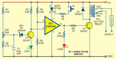
The circuit uses IC CA3140 (IC1) as a voltage comparator to detect voltage changes in the unregulated power supply due to AC mains. Mains voltage changes in the primary as also the secondary winding of the transformer, which is sensed by IC1 to energise/de-energise the relay. Zener diode ZD1 provides a reference voltage of 3V to make transistor T1 conduct. Preset VR1 adjusts the breakdown point of ZD1.

Fig. 1: Power supply circuit with resume indicator

Eletronics Circuit Diagrams

When the voltage level is normal, zener diode ZD1 breaks down and transistor T1 is forward-biased. Capacitor C1 provides time delay of a few seconds to avoid any fluctuation affecting the device during power-on. When transistor T1 conducts, the inverting input (pin 2) of IC1 goes low. However, IC1 does not give a high output as its power supply depends on the conduction of SCR1 (BT169). So manual operation is necessary to energise the relay.

When push-to-on swish S1 is pressed, SCR1 fires to provide voltage to IC1 at its pin 7. As the voltage level at the non-inverting input (pin 3) of IC1 is half of the supply voltage, its output becomes high and the relay (RL1) energises. LED2 glows to indicate the high output of IC1 and activation of relay.

When the line voltage goes below 180V, the secondary voltage of the transformer also drops, say, below 12 volts, ZD1 cease to conduct and the collector of T1 becomes high. This high voltage at the inverting input (pin 2) of IC1 makes its output low. The relay de-energises to stop power to the device.

Fig. 2:  Low-voltage Protector Circuit Diagram

Eletronic Circuit Diagrams

Assemble the circuit on a general-purpose PCB and enclose in a suitable cabinet. Use a 12V PCB-mounted relay. Provide holes for LEDs and switch S1 on the front side of the case. Connect AC power voltage to the motor (load) through the common and normally-open (N/O) contacts of the relay. After assembly and checking the circuit, switch on the circuit and wait for a few minutes. LED1 will gradually become bright due to the charging of capacitor C1. Press S1 to energise the relay. Adjust VR1 so as to make LED1 fully on. This will allow easy latching of the relay.

Read More..

Generating Long Time Delays

Generating long delays of several hours can be accomplished by using a low frequency oscillator and a binary counter as shown below. A single Schmitt Trigger inverter stage (1/6 of 74HC14) is used as a squarewave oscillator to produce a low frequency of about 0.5 Hertz. The 10K resistor in series with the input (pin 1) reduces the capacitor discharge current through the inverter input internal protection diodes if the circuit is suddenly disconnected from the supply.

Generating Long Time Delays Circuit diagram


This resistor may not be needed but is a good idea to use. The frequency is divided by two at each successive stage of the 12 stage binary counter (CD4040) which yields about 1 hour of time before the final stage (Q12) switches to a high state. Longer or shorter times can be obtained by adjusting the oscillator frequency or using different RC values.

Each successive stage changes state when the preceding stage switches to a low state (0 volts), thus the frequency at each stage is one half the frequency of the stage before. Waveform diagrams are shown for the last 3 stages. To begin the delay cycle, the counter can be reset to zero by momentarily connecting the reset line (pin 11) to the positive supply. Timing accuracy will not be as good as with a crystal oscillator and may only be around 1 or 2% depending on the stability of the oscillator capacitor.
Read More..

300m FM Transmitter

This fm transmitter circuit is very simple and it has a acceptable transmission . The signal transited from this fm transmitter circuit can be received at almost 300 meters in open air .The circuit require a 3volts operating voltage and can be tuned anywhere in the FM band.The coil should be about 3mm in diameter and 5 turns. The wire is tinned copper wire, 0.61 mm in diameter.

300m FM Transmitter Circuit diagram

After the coil in soldered into place spread the coils apart about 0.5 to 1mm so that they are not touching. If you don’t have a trim cap you can use a fixed value capacitor and you can vary the TX frequency by adjusting the spacing of the coils or placing a small piece of ferrite inside the coil , but the better way to change the transmission frequency is to use a variable capacitor .Connect a half or quarter wavelength antenna (length of wire) to the aerial point. At an FM frequency of 100 MHz these lengths are 150 cm and 75 cm respectively.
Read More..

Sunday, September 1, 2013

AM Radio Receiver Using by TEA5551T

Using TEA5551T monolithic integrated radio circuit can be designed a AM radio receiver circuit which is designed for use as a portable radio receiver with headphones . 

AM Radio Receiver Circuit diagram

The TEA5551T radio receiver circuit contains all is needed for a AM radio receiver circuit (a complete AM part and dual AF amplifier with low quiescent current).The TEA5551T support a input voltage range (VS) from 1.8 V to 4.5 V but the typical voltage is 3 volts .Because in most case we don’t find to buy inductors you need to build the inductors L1 , L2 , L3 . In the picture bellow you can see the construction data for these three inductors .
Read More..

Miniature FM Transmitter

Miniature FM Transmitter Circuit Diagram 

Notes:
The default for the capacitors type is ceramic, preferably the npo 1% (low noise) type or equivalent. But basically nothing critical here. Use any capacitor you have laying around, but NO electrolytic or tantalum caps. Only if you intend to use this circuit outside the home you may want to select more temperature stable capacitors.

To find the signal on your receiver, make sure there is a signal coming into the microphone, otherwise the circuit wont work. I use an old mechanical alarm clock (you know, with those two large bells on it). I put this clock by the microphone which picks up the loud tick-tock. Im sure you get the idea... Or you can just lightly tap the microphone while searching for the location of the signal on your receiver.
Read More..

Wideband Two Pole High Pass Filter Schematic

The circuit provides a 10MHz cutoff frequency. Resistor R3 ensures that the input capacitance of the amplifier does not interact with the filter response at the frequency of interest. An equivalent low pass filter is similarly obtained by capacitance and resistance transformation.

Wideband Two-Pole High-Pass Filter Schematic


Read More..

6W Four Channel LED Driver

CAT4106 is an integrated Four channel LED driver (multi-channel LED driver) and high power dc-dc converter suitable for powering backlighting applications up to a total of 6 watts. Up to four matched LED strings can be accurately programmed with uniform drive current set by a single external resistor. The CAT4106 Four channel LED driver automatically adjusts the output voltage to drive the highest forward voltage string with the minimum headroom voltage maximizing the efficiency.

6W Four Channel LED Driver Circuit diagram


High resolution dimming control is achieved by the EN/PWM logic pin which supports multiple frequencies. This ensures precise PWM dimming control while the device remains fully biased. In addition, when held at logic low, the device to enter a full shutdown zero current mode. External programming resistors set the minimum and maximum voltage limits for the acceptable window of operation for LED strings. Any channel which fails to regulate within the window (Open or Short LED) is detected and flagged on the FAULT logic output (active low, open-drain).

Main features of CAT4106 led driver are : four LED channels with tight current matching , integrated dc-dc boost converter , up to 6 W LED total output power , up to 92% efficiency , low dropout LED channels (500 mV at 175 mA) , high frequency PWM interface (up to 2 kHz) ,adjustable short/open LED detection The CAT4106 requires small ceramic capacitors of 1 μF on the VIN pin (C1), 4.7 μF on the inductor input (C2), and 10 μF on the output (C3). Under normal condition, a 4.7 μF input capacitor (C2) is sufficient. A 47 μH inductor is recommended with current rating of 1 A or higher and 1A rated Schottky diode .

A typical value for resistor R7 and R5 is around 20 kΩ. R6 and R4 can be calculated as follows:


Read More..