Tuesday, April 30, 2013

Build 16 Stage Bi Directional LED Sequencer

The bi-directional sequencer uses a 4 bit binary up/down counter (CD4516) and two "1 of 8 line decoders" (74HC138 or 74HCT138) to generate the popular "Night Rider" display. A Schmitt Trigger oscillator provides the clock signal for the counter and the rate can be adjusted with the 500K pot. Two additional Schmitt Trigger inverters are used as a SET/RESET latch to control the counting direction (up or down). Be sure to use the 74HC14 and not the 74HCT14, the 74HCT14 may not work due to the low TTL input trigger level. When the highest count is reached (1111) the low output at pin 7 sets the latch so that the UP/DOWN input to the counter goes low and causes the counter to begin decrementing.

 When the lowest count is reached (0000) the latch is reset (high) so that the counter will begin incrementing on the next rising clock edge. The three lowest counter bits (Q0, Q1, Q2) are connected to both decoders in parallel and the highest bit Q3 is used to select the appropriate decoder. The circuit can be used to drive 12 volt/25 watt lamps with the addition of two transistors per lamp as shown below in the section below titled "Interfacing 5 volt CMOS to 12 volt loads"

Circuit diagram

Read More..

Saturday, April 13, 2013

1KHz Sinewave Generator

Simple circuitry, low distortion, battery operated Variable, low impedance output as a lot as 1V RMS

Circuit diagram

Parts:

  • R1 5K6 1/4W Resistor
  • R2 1K8 1/4W Resistor
  • R3,R4 15K 1/4W Resistors
  • R5 500R 1/2W Trimmer Cermet
  • R6 330R 1/4W Resistor
  • R7 470R Linear Potentiometer
  • C1,C2 10nF 63V Polyester Capacitors
  • C3 100µF 25V Electrolytic Capacitor
  • C4 470nF 63V Polyester Capacitor
  • Q1,Q2 BC238 25V 100mA NPN Transistors
  • LP1 12V 40mA Lamp (See Notes)
  • J1 Phono chassis Socket
  • SW1 SPST Slider Switch
  • B1 9V PP3
  • Clip for 9V PP3 Battery

Circuit description:

This circuit generates a excellent 1KHz sinewave the utilization of the inverted Wien bridge configuration (C1-R3 & C2-R4). Features a variable output, low distortion and low output impedance in order to get maintain of good overload capability. A small filament lamp ensures a steady long term output amplitude waveform. Useful to test the Audio Millivoltmeter, Audio Power Meter and different audio circuits published in this website online.

Notes:

  • The lamp should be a low current kind (12V 40-50mA or 6V 50mA) to be able to receive excellent long term stability and low distortion.
  • Distortion @ 1V RMS output is zero.15% with a 12V 40mA lamp, raising to zero.5% with a 12V 100mA one.
  • Using a lamp differing from specifications may require a transformation in R6 worth to 220 or one hundred fifty Ohms to make certain right kind circuits oscillation.
  • Set R5 to learn 1V RMS on an Audio Millivoltmeter related to the output with R7 totally clockwise, or to view a sinewave of two.828V Peak-to-Peak on the oscilloscope.
  • With C1,C2 = 100nF the frequency generated is 100Hz and with C1,C2 = 1nF frequency is 10KHz however R5 is wanting adjustment.
  • High acquire transistors most popular for better performance.
Read More..

SW Converter for Digital AM Car Radio

This circuit is purposely offered with many bathroomse ends (not actually, of course) to stimulate experimenting with RF circuitry at a small outlay. Looking at the circuit diagram you could additionally recognize a modified model of the SW Converter for AM Radios described in different situations in that issue. The changes had been necessary to make the circuit compatible with a digital quite than analogue AM car radio. The main distinction between digital AM radios and their all-analogue predecessors is that tuning is in 9 kHz (some-times 4.5 kHz steps) in compliance with the international frequency allocation for the band. Obviously, that exact step dimension, fascinating as it can be on MW, is a stumbling block if you want to use a digital AM receiver together with a frequency step-up converter for SW, where chaos reigns and there isn't any fastened step dimension. The first try was once to make the crystal oscillator variable through about 5 kHz each and every approach.
 
Circuit diagram :
SW Converter for Digital AM Car Radio Circuit Diagram
 
Unfortunately, regardless of serious efforts, the crystal could not be pulled more than 1 or 2 kHz so some different resolution had to be found. After finding out the NE/SA602/612 informationsheet, it was once found that a variable LC based totally oscillator was once one of the best different. The circuit labored after winding a resonant LC circuit and including a zero.1 µF sequence capacitor to dam the DC element on pin 6 of the NE602 (612). When the tuning used to be found to be a bit sharp with the original capacitor, a simple bandspread (or advantageous tuning) characteristic used to be added via shunting the LC resonant circuit with a lightly loaded 365 pF tuning capacitor (C10) which, like the principle tuning counterpart, C8, was once ratted from an outdated transistor radio. The tuning coil, L1, consists of 8 to 10 turns of 0.6-0.8mm dia. enamelled copper wire (ECW) on a 6-8 mm dia. former with out a core. With this coil, frequency protection shall be from about 4 MHz to 12 MHz or so. Details on Tr1 may be discovered in the referring article.
 
Note that no tuning capacitor is used on the secondary — the input stray capacitance of the NE602 (612) does the trick. A BFO (beat frequency oscillator) was once delivered to let SSB (single sideband) signals to be received. The BFO built round T1 is inconspicuous, has a heap of output and that is steady enough to automobilery an SSB signal for a few minutes with out adjustment. The BFO frequency is tuned with C3. Tr2 is a ready-made four55 kHz IF transformer whose inner capacitor was once first crushed after which eliminated with pliers. When S2 is closed the BFO output sign is solely superimposed on the NE602 (612) IF output to the MW radio. The converter will have to be built into a steel box for shielding. If you in finding that the BFO provides too much output, disconnect it as steered in the circuit diagram and let stray coupling do the work. Sensitivity, even on a 1-metre size of automotive radio aerial, is quite superb. Bearing in mind that many of the main international SW broadcasting stations like Radio NHK Japan, Moscow, BBC and many others.) generate enough power to ensure that you are going to hear them, it's nonetheless kind of thrilling to pay attention to such signals for the first time in your automobile radio. 


http://www.ecircuitslab.com/2012/02/sw-converter-for-digital-am-car-radio.html
Read More..

Reservoir Pump Controller

This circuit operates an automotive windscreen washer pump to fill a 20-litre drum from a 205-litre water reservoir. The drum is suspended above a drip line, which irrigates a vegetable backyard. Two chrome steel probes established within the drum act as sensors for the device. One probe is positioned at the excessive water mark, the other at about half-full. The pump power is switched with the aid of a 12V automotive relay (RLY1). Two op amps (IC1a & IC1b) linked as voltage comparators form the basis of the circuit. 

Initially, assume a falling water stage with the pump switched off. When the water level exposes the decrease probe, the non-inverting input (pin 5) of IC1b rises to about 7.4V. With trimpot VR2 correctly adjusted, this can be higher than the voltage on pin 6. The output (pin 7) therefore swings excessive, biasing Q1 into habitsion. This in turn result ins Q4 to behavior, switching on the relay and starting the pump. 

In addition, when Q4 switches on it supplies base current to Q3 by manner of a 6.8kO resistor. Initially, this current wafts throughout the 47µF capacitor, but once its base-emitter voltage reaches about zero.6V, Q3 behaviors. This action latches Q4 in the \"on\" state, because its base present can go with the flow to floor by implys of Q3 when Q1 ceases behavioring – on the method in which to occur when the rising water stage reaches the low probe. When the water degree reaches the high probe, the voltage on the non-inverting enter (pin 2) of IC1a decreases markedly as a outcome of the habitsivity of the water.

Circuit diagram:

Reservoir Pump Controller Circuit Diagram

If trimpot VR1 is appropriately adjusted, the output (pin 1) swings excessive, switching on Q2. This discharges the 47µF capacitor and robs Q3 of its base present, switching this transistor off. This in flip switches off Q4 and the relay. The zener diodes and 1kO collection resistors at the probe enters protect the op amp’s high impedance inputs from the effects of static discharge. The 47µF capacitor in parallel with the base-emitter junction of Q1 prevents the latching operate from being activated when energy is utilized to the circuit. The author’s setup is energyed from an previous car battery charged from a 12V solar panel.

http://www.ecircuitslab.com/2011/08/reservoir-pump-controller.html
Read More..

Friday, April 12, 2013

230 V AC To 400 V DC Power Supply Circuit Diagram


Description

               A lot of students are who dont know the highest method to convert 230 volt AC to 400 DC. So today i am printed   230 V AC to 400 V DC circuit diagram on my blog. Working idea of this circuit diagram is very simple. You already knew the working theory of a bridge rectifier. This circuit is related as bridge rectifier and the working concept can be related. The fuse is used to supply safety to the circuit, if the current is greater than 1 A.

Parts List

Component No:Value
F11 A
B1IN4007 
C1470MF/450V 
V1230 V AC 
Read More..

LED Multicolour Backlights

This circuit comprises two parts: a string of 5mm high-intensity white LEDs connected in series and the circuit wired around. IC CD4060 with an inbuilt oscillator. The IC is wired such that its outputs Q4, Q5 and Q6 are chosen for colour display. On power-’on’ reset, these outputs go ‘high’ simultaneously but for different time durations. The Q4 output goes ‘high’ for about 18 seconds, Q5 about 38 seconds and Q6 about 80 seconds. These outputs are connected to forty 5mm LEDs through transistors T1, T2 and T3.

It is necessary to boost the current because LEDs are connected in parallel. To do so, transistor BD135 is used. The 1.2-kilo-ohm base resistor prevents overloading of BD135. The 100-ohm resistor acts as the current limiter. Provide heat-sink to each BD135 transistor. LEDs of three colours—blue, orange and red—are used here.
LED Multicolour Backlights
Fig. 1: Circuit for multicolour curtain backlight
To reduce the time duration for which IC outputs go high, replace 2.2-mega-ohm resistor (R4) with 1 mega-ohm. Replace 2.2-mega-ohm resistor with 3.9 mega-ohms to increase the time duration. Power supply for the IC is provided by 220V AC to 9V, 1.5A step-down transformer after rectification and filtering.

A combination of different colours results due to switching on of transistors T1 through T3 for different time durations. These colours with a white background create a beautiful display. The first group of LEDs lights up a few seconds after power to the circuit is switched ‘on.’

Fig. 2: Arrangement of LEDs
Read More..

Shortwave SW Transmitter Based IC BEL1895


Here the SW transmitter circuit based on IC BEL1895. This particular transmitter circuit works in shortwave HF band (6 MHz to 15 MHz), and can be applied for shortrange communication and for educational purposes.

Shortwave (SW) Transmitter Circuit diagram :


The circuit is composed of a mic amplifier circuit, a variable frequency oscillator, and modulation amplifier stages. Transistor T1 (BF195) is put to use as a simple RF oscillator. Resistors R6 and R7 determine base bias, while resistor R9 is utilized for stability. Feedback is provided by 150pF capacitor C11 to maintain oscillations. The primary of shortwave oscillator coil and variable condenser VC1 (365pF, 1/2J gang) form the frequency determining network.

By altering the coil inductance or the capacitance of gang condenser, the frequency of oscillation can be modified. The carrier RF signal from the oscillator is inductively coupled through the secondary of transformer X1 to the next RF amplifier-cum-modulation stage assembled around transistor T2 that is run in class ‘A’ mode. Audio signal from the audio amplifier assembled around IC BEL1895 is coupled to the emitter of transistor 2N2222 (T2) for RF modulation.

IC BEL1895 is a monolithic audio power amplifier intendeded for sensitive AM radio applications. It can deliver 1W power to 4 ohms at 9V power supply, with low distortion and noise characteristics. Since the amplifier’s voltage gain is of the order of 600, the signal from condenser mic can be straightly linked to its input without any amplification.

The transmitter’s stability is managed by the quality of the tuned circuit parts as well as the degree of regulation of the supply voltage. A 9V regulated power source is required. RF output to the aerial consists of harmonics, because transistor T2 doesn’t have tuned coil in its collector circuit. However, for short-range communication, it does not create any trouble. The harmonic content of the output may be lowered by means of a high-Q L-C filter or resonant L-C traps tuned to each of the prominent harmonics. The power output of this transmitter is about 100 milliwatts.
Read More..

15 6 Inch Laptop Mocha ASUS A53Z AS61

ASUS A53Z-AS61 15.6-Inch Laptop (Mocha)

Uncompromised Quality and Unique facial appearance with Affordability appearing in Mind
Ideal pro individuals who seek a highly unswerving notebook for creation otherwise drama devoid of contravention the shore, the ASUS A succession is the achieve preference. With unique skin texture and technologies, it is the ultimate solution meant for your productivity and entertainment needs while on-the-proceed.

Tried and Tested for Quality
ASUS is a worldwide tools leader who focuses on the mastery of innovation and design perfection. these days, it is the globes #1 manufacturer of motherboards and is lone of the humanitys top PC brands. ASUS embodies the passion to create products to correctly enhance the computing experience. ASUS products are as well firmly quality tested to improve on industry values, surviving multiple trickle tests, center tests cycles and LCD pressure tests, ensuring to facilitate each ASUS effect you bad deal command stay individual of your greatest reserves.

Reliability Matters
ASUS PCs conclude bordering on otherwise by the top of the industrys reliability rankings survey in the same way as survey1

Recognized in lieu of their unequaled reliability, ASUS products evidently offers you amity of mind and quality you can trust. Using premium equipment, ASUS aims to break the industry mold and supply a manufactured goods with the intention of is in all honesty incredible. taking part in addition, ASUS furthermore offers the industrys top-in-group of pupils complimentary warranty and on the house 1-day unintended hurt protection so you can doze apprehension-free knowing ASUS has your back.

Innovation like no other
Designed with you in mind, ASUS equipped the A cycle with innovative technologies with the aim of fit your needs. on behalf of illustration, IceCool expertise helps keep the palm support cool even later prolonged enjoy. ASUS Palm impervious knowledge prevents not premeditated indicator movement on the track pad once typing, thus only if better accuracy while bowdlerization before lettering a article.

The ASUS A sequence delivers an immersive multimedia experience through its important-definition LED panel and SRS Premium Sound via Altec Lansing speakers. Log in the field of to your laptop password-emancipated with SmartLogon facial recognition knowledge. Plus, it offers reconciliation of mind preventing redundant access by other associates, saving you occasion and keeping your laptop secure.

Technical Details 15.6-Inch Laptop (Mocha) | ASUS A53Z-AS61
Technical Details 15.6-Inch Laptop (Mocha) | ASUS A53Z-AS61

Read More..

Build LM1812 Ultrasonic Transceiver

The LM1812 is a complete ultrasonic transceiver on a chip designed for use in a variety of pulse-echo ranging applications. The chip operates by transmitting a burst of oscillations with a transducer, then using the same transducer to listen for a return echo. Ifan echo of sufficient amplitude is received, the LM1812 detector puts out a pulse of approximately the same width as the original burst. The closer the reflecting object, the earlier the return echo. 

Ultrasonic-Transceiver Circuit Diagram
Ultrasonic-Transceiver-Circuit-Diagram1

Echos could be received immediately after the initial burst was transmitted, except for the fact that the transducer rings. When transmitting, the transducer is excited with several hundred volts peak to peak, and it operates in a loudspeaker mode. Then, when the LM1812 stops transmitting and begins to receive, the transducer continues to vibrate or ring, even though excitation has stopped. The transducer acts as a microphone and produces an ac signal initially the same amplitude as the transmit pulse. This signal dies away as is governed by the transducer"s damping factor, but as long as detectable ringing remains, the LM1812"s detector will be held on, masking any return echos.Link
Read More..

Thursday, April 11, 2013

Light and Dark Dependent Circuir

This is the circuit of a simple buzzer
that is activated by darkness, the buzzer is off when theres light and
on when it is dark. A general-purpose operational amplifier, the 741, is
used as a comparator that determines whether it is dark enough to turn on a self-oscillating piezoelectric buzzer.
Its inverting input is connected to a photoresistor,
a component whose resistance decreases as more light shines on it.  Its
non-inverting input, on the other hand, is connected to an almost fixed
voltage, i.e., a proportion of the supply voltage as set by timmer
resistor R2. 
 
Figure 1.  Darkness-Activated Buzzer Circuit Diagram.

            If there is ample light shining on the photo-resistor, the buzzer is quiet. As less light shines on the photo-resistor,
its resistance increases and causes the voltage across R1 to decrease. 
At a certain level of lighting, the voltage across R1, which is also
the voltage at the inverting input of the 741, becomes smaller than the
voltage at the non-inverting input. At this point, the 741 is triggered
to output a high level, turning on Q1.  Q1 then activates the
self-oscillating piezoelectric buzzer.
Read More..

RF Amplifier circuit with 2SC1970 2N4427

RF power amplifier circuit of this work is based on the transistor 2SC1970 and 2N4427. The set output power of 88-108 MHz FM RF Amplifier With 2SC1970 is about 1.3W and the input driver is 30-50mW. RF driver amplifier circuit uses a 2N4427 and its power amplifier using a transistor 2SC1970.

At the time of the amplifier circuit tuning FM 88-108 MHz RF Amplifier With 2SC1970 should use the power meter / watt meter or SWR or RF field can also use the meter. RF amplifier circuit can work from the frequency of 88-108 MHz.

RF Amplifier

Circuit of 88-108 MHz FM RF Amplifier With RF 2SC1970 can radiate far enough. At the time of tuning you should use a 50 Ohm dummy load. For the input signal should be installed to regulate the VR level so as not to over-modulation (30-50mW).
Read More..

PC Power Saver

This circuit is designed to help minimise the  quiescent power consumption of PCs and  notebooks, using just our old friend the 555  timer and a relay as the main components. The  circuit itself dissipates around 0.5 W in operation (that is, when the connected PC is on);  when switched off (with the relay not energised) the total power draw is precisely zero. A prerequisite for the circuit is a PC or note book with a USB or PS/2 keyboard socket that  is powered only when the PC is on. The power saver can be used to switch PCs  or even whole multi-way extension leads. The unit can be built  into  an  ordinary  mains  adaptor (which must have an earth  pin!) as the photograph of the  author‘s prototype shows. The  PC is plugged in to the socket  at the output of the power saver  unit, and an extra connection  is made to the control input of  the unit from a PS/2 (keyboard or mouse) socket or USB port. Only  the 5 V supply line of the interface is used.
 
PC Power Saver Image  
PC Power Saver Image

When button S1 on the power saver  is pressed the unit turns on, and the  monostable formed by the 555 timer is  triggered via the network composed by  R4 and C7. This drives relay RE1, whose contacts close. The connected PC is now tentatively powered up via the relay for a period  determined  by  P1  (approximately in the range from 5 s to 10 s). If, during this interval, the PC fails to indicate  that it is alive by supplying 5 V from its USB or  PS/2 connector (that is, if you do not switch  it on), the monostable period will expire, the  relay will drop out and any connected device  will be powered down. No further current will  be drawn from the supply, and, of course, it  will not be possible to turn the PC on. When-ever you want to turn the PC on, you must  always press the button on the power saver  shortly beforehand. 

If, however, 5 V is delivered by the PC to the  input of optocoupler IC2 before the monostable times out (which will be the case if the  PC is switched on during that period), the  transistor in the optocoupler will conduct  and discharge capacitor C6. The monostable  will now remain triggered and the relay will  remain energised until the PC is switched off  and power disappears from its USB or PS/2  interface. Then, after the monostable time  period expires, the relay will drop out and the  power saver will disconnect itself from the mains. There is no need to switch anything  else off: just shut down the system and the  power saver will take care of the rest.
 
Circuit diagram :
PC Power Saver-Circuit-Diagram
PC Power Saver Circuit Diagram
 
It is also  possible to leave the machine as it updates its  software, and the power saver will do its job  shortly after the machine shuts down. Power for the unit itself is obtained using a  simple supply circuit based around a miniature transformer. Alternatively, a 12 V mains  adaptor can be used, as long as a relay with a  12 V coil voltage is used for RE1. In his proto-type the author used a relay with a 24 V coil  connected as shown directly to the positive  side of reservoir capacitor C2, the 555 being  powered from 12 V regulated from that sup-ply using R1 and D1. A fixed resistor can of  course be used in place of P1 if desired. If the  adjustment range of P1 is not sufficient (for  example if the PC powers up very slowly) the  monostable period can be increased by using  a larger capacitor at C6.  The relay must have at least two normally-open (or changeover) contacts rated at at  least 8 A. The contact in parallel with S1 is used to supply power to the device  itself, and the other contact carries  all the current for the connected  PC  or  for  the  ex tension  lead  to  which  the  PC  and  peripherals  are  connected. 

Pushbutton S1 must be rated for 230 VAC  (US: 120 VAC) operation: this is no place to  make economies. The coil current for the relay  flows through LED D5, which must therefore  be a 20 mA type. If a low-current LED is used,  a 120 Ω resistor can be connected in parallel with it to carry the remaining current.  The Fujitsu FTR-F1CL024R relay used in the  author’s prototype has a rated coil current of  16.7 mA. Optocoupler IC2 provides isolation between  the circuit and the PC, and is protected from  reverse polarity connection by diode D4. The power saver should be built into an insulated enclosure and great care should be  taken to ensure that there is proper isolation  between components and wires carrying the  mains voltage and the other parts of the circuit. In particular, the connection to the PC  and associated components (R6, C5, D4 and  IC2) should be carefully arranged with at least  a 6 mm gap between them and any part of  the circuit at mains potential. 


Source by : Streampowers.blogspot.com
Read More..

Digital Step Km Counter

This circuit measures the distance covered during a walk. Hardware is located in a small box slipped in pants pocket and the display is conceived in the following manner: the leftmost display D2 (the most significant digit) shows 0 to 9 Km. and its dot is always on to separate Km. from hm. The rightmost display D1 (the least significant digit) shows hundreds meters and its dot illuminates after every 50 meters of walking. A beeper (excludable), signals each count unit, occurring every two steps. A normal step was calculated to span around 78 centimeters, thus the LED signaling 50 meters illuminates after 64 steps (or 32 operations of the mercury switch), the display indicates 100 meters after 128 steps and so on.

For low battery consumption the display illuminates only on request, pushing on P2. Accidental reset of the counters is avoided because to reset the circuit both pushbuttons must be operated together. Obviously, this is not a precision meter, but its approximation degree was found good for this kind of device. In any case, the most critical thing to do is the correct placement of the mercury switch inside of the box and the setting of its sloping degree.
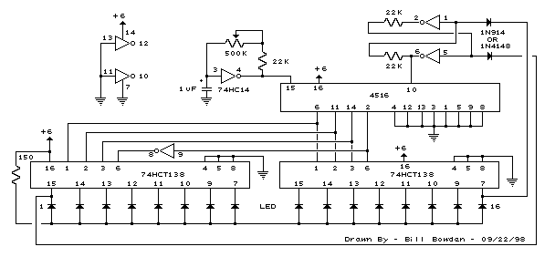
Circuit diagram:
digital_step_km_counter_circuit_diagram
Digital Step-Km Counter Circuit Diagram

Parts:
R1 = 22K 1/4W Resistor
R2 = 2.2M 1/4W Resistor
R3 = 22K 1/4W Resistor
R4 = 1M 1/4W Resistor
R5 = 4.7K 1/4W Resistor
R6 = 47R 1/4W Resistor
R7 = 4.7K 1/4W Resistor
R8 = 4.7K 1/4W Resistor
R9 = 1K 1/4W Resistor
C1 = 47nF 63V Polyester Capacitor
C2 = 100nF 63V Polyester Capacitor
C3 = 10nF 63V Polyester Capacitor
C4 = 10µF 25V Electrolytic Capacitor
D1 = Common-cathode 7-segment LED mini-display (Hundreds meters)
D2 = Common-cathode 7-segment LED mini-display (Kilometers)
Q1 = BC327 45V 800mA PNP Transistors
Q2 = BC327 45V 800mA PNP Transistors
P1 = SPST Pushbutton (Reset)
P2 = SPST Pushbutton (Display)
IC1 = 4093 Quad 2 input Schmitt NAND Gate IC
IC2 = 4024 7 stage ripple counter IC
IC3 = 4026 Decade counter with decoded 7-segment display outputs IC
IC4 = 4026 Decade counter with decoded 7-segment display outputs IC
SW1 = SPST Mercury Switch, called also Tilt Switch
SW2 = SPST Slider Switch (Sound on-off)
SW3 = SPST Slider Switch (Power on-off)
BZ = Piezo sounder
B1 = 3V Battery (2 AA 1.5V Cells in series)

Circuit operation:

IC 1A & IC 1B form a monostable multi vibrator providing some degree of freedom from excessive bouncing of the mercury switch. Therefore a clean square pulse enters IC2 that divides by 64. Q2 drives the LED dot-segment of D1 every 32 pulses counted by IC2. Either IC3 & IC4 divide by 10 and drive the displays. P1 resets the counters and P2 enables the displays. IC1C generates an audio frequency square wave that is enabled for a short time at each monostable count. Q1 drives the piezo sounder and SW2 allows disabling the beep.

Notes:
  • Experiment with placement and sloping degree of mercury switch inside the box: this is very critical.
  • Try to obtain a pulse every two walking steps. Listening to the beeper is extremely useful during setup.
  • Trim R6 value to change beeper sound power.
  • Push P1 and P2 to reset.
  • This circuit is primarily intended for walking purposes. For jogging, further great care must be used with mercury switch placement to avoid undesired counts.
  • When the display is disabled current consumption is negligible, therefore SW3 can be omitted.

Streampowers
Read More..

1979 Jeep CJ Electrical Wiring Diagram

1979 Jeep CJ Elecrical Wiring Diagram
The part of 1979 Jeep CJ Electrical Wiring Diagram: accessory feed, air conditioner compressor, anti diesel solenoid, back up lamps, manual transmission, battery, boy, brake, cogar lighter, capacitor, chassis, marker & reflector, module assembly, neutral safety switch, oil lamp gauge, oil pressure sender, panel lamp, parking brake, park & signal lamp, resistor heater blower moor, splice, coil 6 cylinder, dimmer switch, distributor, electric choke, fuel gauges, fuel sender, ground fan lamp feed, headlamp, heater motor, ignition switch, horn relay, kick down, starting motor, stop lamp, tail & stop lamp, temperature gauge, temperature sender, windshield wiper, washer.
Read More..

Wednesday, April 10, 2013

Threadwiring Clipsal Saturn Light Switches

House Wiring on Telephone Socket Wiring   How To Do It
Telephone Socket Wiring How To Do It.


House Wiring on Thread  Wiring Clipsal Saturn Light Switches
Thread Wiring Clipsal Saturn Light Switches.


House Wiring on Mesa Whole House Wiring Services Provided By Amadeus Electric
Mesa Whole House Wiring Services Provided By Amadeus Electric.


House Wiring on Russell Residence  10007 Meadow Road Sw  Lakewood Wa 98499
Russell Residence 10007 Meadow Road Sw Lakewood Wa 98499.


House Wiring on Home House Wiring Installation
Home House Wiring Installation.


House Wiring on Wiring A Switched Outlet Wiring Diagram   Electrical Online
Wiring A Switched Outlet Wiring Diagram Electrical Online.


House Wiring on Wiring A Light Switch For A Ceiling Light Diy Project
Wiring A Light Switch For A Ceiling Light Diy Project.


House Wiring on In A Home Equipped With Lexcom Home Wiring Network Cabling System
In A Home Equipped With Lexcom Home Wiring Network Cabling System.


House Wiring on House Wiring Cable
House Wiring Cable.


House Wiring on Ted Displays Up To The Second Energy Use And Cost Information In An
Ted Displays Up To The Second Energy Use And Cost Information In An.


Read More..

Low Forward Drop Rectifier schematic

A
TMOS power FET , Q1 , and LM393 comparator provide a high efficiency
rectifier circuit. When Va exceeds Vb1 U1s output becomes high and Q1
conducts. Conversely, when Vb exceeds Va1, the comparator output
becomes low and Q1 does not conduct.
Low forward dopr schematic
The
Forward drop is determined by Q1s on resistance and current I. The
MTH40N05 has an ON resistance of 0.028 Ω ; for I = 10 A , the forward
drop is less than 0.3V .Typically , the best Schottky diodes do not even
begin conducting below a few hundred mV.
Read More..

Build Permanent Magnet Motor Chatroulettehof

Smith Motors Wiring Diagram on Here S The Wiring Diagram For Your Motor W O Generator   Ajilbab Com
Here S The Wiring Diagram For Your Motor W O Generator Ajilbab Com.


Smith Motors Wiring Diagram on How To Wire Up 115v 2 Speed 1 Hp A O  Smith Motor     Above Ground
How To Wire Up 115v 2 Speed 1 Hp A O Smith Motor Above Ground.


Smith Motors Wiring Diagram on 01   A O Smith Centurion Square Flange Pool Pump Motor  0 75 Hp
01 A O Smith Centurion Square Flange Pool Pump Motor 0 75 Hp.


Smith Motors Wiring Diagram on Build Permanent Magnet Motor Http Chatroulettehof Com What Is The Ics
Build Permanent Magnet Motor Http Chatroulettehof Com What Is The Ics.


Smith Motors Wiring Diagram on Small Ac Electric Motors Ultimate Washer Customer Id Top Quality Small
Small Ac Electric Motors Ultimate Washer Customer Id Top Quality Small.


Smith Motors Wiring Diagram on My Blower Motor Went Out Today And I Bought A New Ao Smith
My Blower Motor Went Out Today And I Bought A New Ao Smith.


Smith Motors Wiring Diagram on 4hp Ao Smith Electric Pool Motor  Hayward  For 56j Fr Motors
4hp Ao Smith Electric Pool Motor Hayward For 56j Fr Motors.


Smith Motors Wiring Diagram on Syncro Gear Module By Us Electric  1 3 Hp Listing  129425
Syncro Gear Module By Us Electric 1 3 Hp Listing 129425.


Smith Motors Wiring Diagram on Click On Picture To Enlarge
Click On Picture To Enlarge.


Smith Motors Wiring Diagram on Motor 5 Hp Century   A O Smith Air Compressor Electric Motor
Motor 5 Hp Century A O Smith Air Compressor Electric Motor.


Read More..

Simple Steam Whistle

This circuit consists of six square wave oscillators. Square waves are made up of a large number of harmonics. If six square waves with different frequencies are added together, the result will be a signal with a very large number of frequencies. When you listen to the result you’ll find that it is very similar to a steam whistle. The circuit should be useful in modelling or even in a sound studio.
Circuit diagram :
Simple Steam Whistle-Circuit Diagram
Simple Steam Whistle Circuit Diagram

This circuit uses only two ICs. The first IC, a 40106, contains six Schmitt triggers, which are all configured as oscillators. Different frequencies are generated by the use of different feedback resistors. The output signals from the Schmitt triggers are mixed via resistors. The resulting signal is amplified by IC2, an LM386. This IC can deliver about 1 W of audio power, which should be sufficient for most applications. If you leave out R13 and all components after P1, the output can then be connected to a more powerful amplifier. In this way a truly deafening steam whistle can be created. The ‘frequency’ of the signal can be adjusted with P2, and P1 controls the volume.


Streampowers
Read More..

Understanding SG3525 IC Pin Outs

The article explains the pin out functions of the IC SG3525 which is a regulating pulse width modulator IC. Lets understand in details:


The main features of the IC SG3525 may be understood with the following points:


  • Operating voltage = 8 to 35V
  • Error amp reference voltage internally regulated to 5.1V 
  • Oscillator frequency is variable through an external resistor within the range of 100Hz to 500 kHz.
  • Facilitates a separate oscillator sync pin out.
  • Dead time control is also variable as per intended specs.
  • Has an internal soft start feature
  • Shut down facility features a pulse by pulse shutdown enhancement.
  • Input under voltage shut down feature also is included.
  • PWM pulses are controlled through latching for inhibiting multiple pulse outputs or generation.
  • Output supports a dual totem pole driver configuration.


SG3525 Pin-Out Description

A practical implementation of the following pin-out data may be understood through this inverter circuit

The IC SG3525 is a single package multi function PWM generator IC, the main operations of the respective pin outs are explained with the following points:

Pin#1 and #2 (EA inputs): These are inputs of the built-in error amplifier of the IC. Pin#1 is the inverting input while pin#2 is the complementary non-inverting input.
Its a simple opamp arrangement inside the IC whose output controls the PWM of the output. Thus these pin outs can be effectively used for correcting the output voltage of a converter.

It may be done by applying a sample voltage from the output through a voltage divider network to the non-inverting input of the opamp (pin#1). The fed voltage should be adjusted to be just below the internal reference voltage value when the output is normal.....now if the output voltage increases, the sample voltage would also increase and at some point exceed the reference limit, prompting the IC to take necessary corrective measures so that the voltage is restricted to the normal level.

Pin#3 (Sync): This pin can be used for synchronizing the IC with an external oscillator frequency. This is generally done when more than a single IC is used and requires to be controlled with a common oscillator frequency.

Pin#4 (Osc. Out): Its the oscillator output of the IC, the frequency of the IC may be confirmed at this pin out.

Pin#5 and #6(Ct, Rt): These are termed Ct, Rt respectively. Basically these pin outs are connected with external resistors and capacitors for setting up the frequency of the inbuilt oscillator stage or circuit. Ct must be attached with a relevant capacitor while the Rt pin with a resistor for optimizing the frequency of the IC.

Pin#7 (discharge): This pin out can be used for determining the dead time of the IC, meaning the time gap between the switching of the two outputs of the IC (A and B). A resistor connected across this pin and ground fixes the dead time of the IC.

Pin#8 (Soft Start): This pin out as the name suggests is used for initiating the operations of the IC in a soft manner instead of a sudden or abrupt jerk. The capacitor connected across this pin and ground decides the level of soft initialization of the output of the IC.

Pin#9 (Comp): This pin out is not so important, just needs to be connected with the INV input of the error amplifier in order to keep the EA operations smooth and without hiccups.

Pin#10 (Shutdown): As the name suggest this pin out may be used for shutting down the outputs of the IC in an event of a circuit malfunction or some drastic conditions. A logic high at this pin out will instantly narrow down te PWM pulses to the maximum possible level making the output devices current go down to minimal levels. However if the logic high persists for longer period of time, the IC prompts the slow start capacitor to discharge, initiating a slow turn ON and release. This pin out should not be kept unconnected for avoiding stray signal pick ups.

Pin#11 and #14 (output A and output B): These are the two outputs of the IC which operate in a  totem pole configuration or simply in a flip flop or push pull manner. External devices which are intended for controlling the converter transformers are integrated with these pin outs for implementing the final operations.

Pin#12 (ground): Its the ground pin of the IV or the Vss.

Pin#13(Vc): The output to A and B are switched via the supply applied to pin#13. This is normally done via a resistor connected to the main DC supply. Thus this resistor decides the magnitude of trigger current to the output devices.

Pin#15 (Vi): Its the Vcc of the IC, that is the supply input pin.

Pin#16: It provides the internal 5.1V reference for optional use. This pint must be terminated with a low value capacitor to ground.


Read More..

Tuesday, April 9, 2013

Analog Signal Transmission Over Telephone Lines

This is a circuit for telephone line is designed to carry audio signal, which is an alternating current in nature. To transmit measurement signal, which has very low frequency or DC signal, we have to convert the signal into AC with acceptable frequency range for telephone line transmission. This is the figure of the block diagram circuit;


For transmitting analog data over telephone lines, its ideal to use the TC9400′s square-wave output. Since the square wave takes up less frequency spectrum a square wave is actually preferred over a pulse waveform for data transmission. By use of low pass filters, the square wave’s spectrum can be further reduced. The TC9400 converts the frequency signal back into a voltage output linearly proportional to the original input voltage at the end of the telephone line. [Block diagram source: Microchip Application Note]
Read More..

Multiplexer

Multiplexer is an electronic circuit that functions to select one among many inputs into one output. The number of bits from the selector (selector) to determine the number of input channels can be received.
With provisions are:

I = 2 ^ s

where:
I: Number of input channels can be received
s: The number of bits of the selector or the number of lines of voters

for example if we want the 14 input channels, then the minimum number of bits of selectors who should we meet is 4 bits. Where is the selector 4 bits can represent 16 channels of input.
Read More..

Fuse Box Ford 2005 Freestyle Diagram

Fuse Box Ford 2005 Freestyle Diagram - Here are new post for Fuse Box Ford 2005 Freestyle Diagram.

Fuse Box Ford 2005 Freestyle Diagram


Fuse Box Ford 2005 Freestyle Diagram

Fuse Panel Layout Diagram Parts: electrical connector, seats, ignition system, instrument cluster.
Read More..

Rj45 Wiring Diagram

Rj45 Wiring Diagram on Rj45 Wiring Diagram
Rj45 Wiring Diagram.


Rj45 Wiring Diagram on Rj45 Wiring Diagrams
Rj45 Wiring Diagrams.


Rj45 Wiring Diagram on Rj45 Pinout Wiring  How To Make Up A 10baset 100baset Connection  Eia
Rj45 Pinout Wiring How To Make Up A 10baset 100baset Connection Eia.


Rj45 Wiring Diagram on Ethernet Wiring Colors
Ethernet Wiring Colors.


Rj45 Wiring Diagram on Ethernet Rj45 Installation Cable Diagram
Ethernet Rj45 Installation Cable Diagram.


Rj45 Wiring Diagram on Structured Wiring Retro   Install 1
Structured Wiring Retro Install 1.


Rj45 Wiring Diagram on Rj45 To Db9 Adapter
Rj45 To Db9 Adapter.


Rj45 Wiring Diagram on Santomieri Systems   Cat 5 Rj45 Wire Diagrams
Santomieri Systems Cat 5 Rj45 Wire Diagrams.


Rj45 Wiring Diagram on Insert The Rj45 Connector Into The Crimping Tool  Again Carefully Make
Insert The Rj45 Connector Into The Crimping Tool Again Carefully Make.


Rj45 Wiring Diagram on Yost Rj45 To Db25 Serial Dce Adapter Wiring
Yost Rj45 To Db25 Serial Dce Adapter Wiring.


Read More..