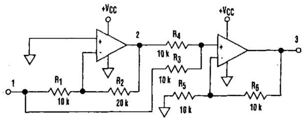
Diode less Rectifier Circuit Diagram . It`s common knowledge that when working with single-supply op amps, implementing simple functions in a bipolar signal environment can be difficult. Sometimes additional op amps and other electronic components are required. Taking that into consideration, can any advantage be attained from this mode The answer lies in this simple circuit (A). Requiring no diodes, the circuit is a high-precision full-wave rectifier with a liigli-frequency limitation equalling that of the op amps themselves. Look at the circuit`s timing diagram (B) to see the principle of operation. The first amplifier rectifies negative input levels with an inverting gain of 2 and turns positive levels to zero .
The second amp, a noninverting summing amplifier, adds the inverted negative signal from the first amplifier to the original input signal. The net result is the traditional waveform produced by full-wave rectification. In spite of the limitation on the input signal amplitude (it must be less than VCCJZ), this circuit can be useful in a variety of setups.
Diode less Rectifier Circuit Diagram

No comments:
Post a Comment
Note: Only a member of this blog may post a comment.