Showing posts with label controlled. Show all posts

Saturday, December 21, 2013

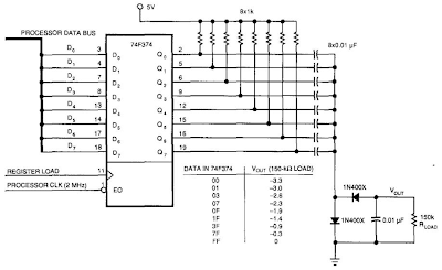
Simple Up Controlled Negative Voltage Converter Circuit Diagram

This Simple Up-Controlled Negative Voltage Converter Circuit Diagram was used to produce a variable negative voltage for contrast control of an LCD display. A 74F374 generates a square wave that is ac coupled to a rectifier and load. By using the uP clock and data from the processor bus, and properly timed load signal, the dc level generated can be controlled by the uP. 

Simple Up-Controlled Negative Voltage Converter Circuit Diagram 

Simple Up-Controlled Negative Voltage Converter Circuit Diagram
 
Read More..

Tuesday, September 3, 2013

Temperature Controlled Fan Circuit

Warning! The circuit is connected to 230Vac mains, then some parts in the circuit board are subjected to lethal potential! Avoid touching the circuit when plugged and enclose it in a plastic box.
Description
Gradually increases speed as temperature increases
Widely adjustable temperature range
Circuit Diagram
Parts:
P1 22K Linear Potentiometer (See Notes)
R1 15K @ 20°C n.t.c. Thermistor (See Notes)
R2 100K 1/4W Resistor
R3,R6 10K 1/4W Resistors
R4,R5 22K 1/4W Resistors
R7 100R 1/4W Resistor
R8 470R 1/4W Resistor
R9 33K 4W Resistor
C1 10nF 63V Polyester Capacitor
D1 BZX79C18 18V 500mW Zener Diode
D2 TIC106D 400V 5A SCR
D3-D6 1N4007 1000V 1A Diodes
Q1,Q2 BC327 45V 800mA PNP Transistors
Q2 BC337 45V 800mA NPN Transistor
SK1 Female Mains socket
PL1 Male Mains plug & cable
Device purpose:
This circuit adopt a rather old design technique as its purpose is to vary the speed of a fan related to temperature with a minimum parts counting and avoiding the use of special-purpose ICs, often difficult to obtain.
Circuit operation:
R3-R4 and P1-R1 are wired as a Wheatstone bridge in which R3-R4 generates a fixed two-thirds-supply "reference" voltage, P1-R1 generates a temperature-sensitive "variable" voltage, and Q1 is used as a bridge balance detector.
P1 is adjusted so that the "reference" and "variable" voltages are equal at a temperature just below the required trigger value, and under this condition Q1 Base and Emitter are at equal voltages and Q1 is cut off. When the R1 temperature goes above this "balance" value the P1-R1 voltage falls below the "reference" value, so Q1 becomes forward biased, pulse-charging C1.
This occurs because the whole circuit is supplied by a 100Hz half-wave voltage obtained from mains supply by means of D3-D6 diode bridge without a smoothing capacitor and fixed to 18V by R9 and Zener diode D1. Therefore the 18V supply of the circuit is not true DC but has a rather trapezoidal shape. C1 provides a variable phase-delay pulse-train related to temperature and synchronous with the mains supply "zero voltage" point of each half cycle, thus producing minimal switching RFI from the SCR. Q2 and Q3 form a trigger device, generating a short pulse suitable to drive the SCR.
Notes:
The circuit is designed for 230Vac operation. If your ac mains is rated at about 115V, you can change R9 value to 15K 2W. No other changes are required.
Circuit operation can be reversed, i.e. the fan increases its speed as temperature decreases, by simply transposing R1 and P1 positions. This mode of operation is useful in controlling a hot air flux, e.g. using heaters.
Thermistor value is not critical: I tried also 10K and 22K with good results.
In this circuit, if R1 and Q1 are not mounted in the same environment, the precise trigger points are subject to slight variation with changes in Q1 temperature, due to the temperature dependence of its Base-Emitter junction characteristics. This circuit is thus not suitable for use in precision applications, unless Q1 and R1 operate at equal temperatures.
he temperature / speed-increase ratio can be varied changing C1 value. The lower the C1 value the steeper the temperature / speed-increase ratio curve and vice-versa.
Author: RED Free Circuit Designs
Source: http://www.redcircuits.com
Read More..

Friday, August 9, 2013

Audio Controlled Mains Switch

It is often useful for audio or video equipment to be switched off automatically after there has been no input signal for a while. The function of the on-off switch in such equipment is then taken over by switch S2 in the accompanying diagram. It remains, however, possible to  switch off manually by means of Si. Automatic  switch-off occurs after there has been no input  signal for about 2 minutes: this delay makes it possible for a new record or cassette to be placed in the  relevant machine.
 
The audio input to the proposed circuit may be  taken from the output of the relevant TV set, amplifier, or whatever. The input earth is held at + 6 V  with respect to the circuit earth by potential divider  Ri-R2-R3-R4. The two 741s function as comparators: the output of ICi goes high when the in- put signal is greater than + 50 mV, whereas the out- put of IC2 goes high when the input signal  becomes more negative than -50 mV. Resistors  R6, R7, and R8 form an OR gate that drives transistor Ti. If the output of either ICi or IC2 is logic  1, Ti conducts.
 
Circuit diagram :
Audio-Controlled-Mains-Switch-Circuit-Diagram
Audio Controlled Mains Switch Circuit Diagram

The 555  operates as a retrigger able monostable,  whose period is determined by Rio and Ci. The  device is triggered when its pin 2 is earthed by the  closing of S2. Its output, pin 3, then remains high  for 1 to 2 minutes, depending on the leakage cur- rent of the 555. 

The monostable resets itself as soon  as the potential across Ci exceeds a certain value.  As long as there is an input signal to the circuit, Ti conducts and Ci remains uncharged. As soon as  the audio signal ceases, Ti switches off, and Ci  charges until the potential across it is sufficient to  reset the 555. The monostable may also be reset by  closing Si, which connects pin 6 of the 555 to + 12 V.
 
Audio-Controlled-Mains-Switch
 
When IC3 is reset, Ci is discharged via its pin 7. Resistor Rrn serves as protection, because without it Ti could short-circuit the supply lines. When the output of IC3 goes high, T2 conducts,  the relay is energized, and the relay contacts switch on the mains voltage as appropriate. To counter the induced potential when the relay contacts close, which could damage T2, diode Di has been connected in parallel with the relay coil.


Source by : Streampowers
Read More..

Tuesday, May 14, 2013

Temperature controlled DC fan


Here is a simple circuit based on two transistors that can be used to control the speed of a 12 V DC fan depending on the temperature.A thermistor (R1) is used to sense the temperature. When the temperature increases the base current of Q1 (BC 547) increases which in turn decreases the collector voltage of the same transistor. Since the collector of Q1 is coupled to the base of Q2 (BD 140), the decrease in collector voltage of Q1 forward biases the Q2 more and so do the speed of the motor. Also, the brightness of the LED will be proportional to the speed of the motor.
Read More..

Friday, April 5, 2013

Audio Controlled Mains Switch

It is often useful for audio or video equipment to be switched off automatically after there has been no input signal for a while. The function of the on-off switch in such equipment is then taken over by switch S2 in the accompanying diagram. It remains, however, possible to  switch off manually by means of Si. Automatic  switch-off occurs after there has been no input  signal for about 2 minutes: this delay makes it possible for a new record or cassette to be placed in the  relevant machine.
 
The audio input to the proposed circuit may be  taken from the output of the relevant TV set, amplifier, or whatever. The input earth is held at + 6 V  with respect to the circuit earth by potential divider  Ri-R2-R3-R4. The two 741s function as comparators: the output of ICi goes high when the in- put signal is greater than + 50 mV, whereas the out- put of IC2 goes high when the input signal  becomes more negative than -50 mV. Resistors  R6, R7, and R8 form an OR gate that drives transistor Ti. If the output of either ICi or IC2 is logic  1, Ti conducts.
 
Circuit diagram :
Audio-Controlled-Mains-Switch-Circuit-Diagram
Audio Controlled Mains Switch Circuit Diagram

The 555  operates as a retrigger able monostable,  whose period is determined by Rio and Ci. The  device is triggered when its pin 2 is earthed by the  closing of S2. Its output, pin 3, then remains high  for 1 to 2 minutes, depending on the leakage cur- rent of the 555. The monostable resets itself as soon  as the potential across Ci exceeds a certain value.  As long as there is an input signal to the circuit, Ti conducts and Ci remains uncharged. As soon as  the audio signal ceases, Ti switches off, and Ci  charges until the potential across it is sufficient to  reset the 555. The monostable may also be reset by  closing Si, which connects pin 6 of the 555 to + 12 V.
 
Audio-Controlled-Mains-Switch

When IC3 is reset, Ci is discharged via its pin 7. Resistor Rrn serves as protection, because without it Ti could short-circuit the supply lines. When the output of IC3 goes high, T2 conducts,  the relay is energized, and the relay contacts switch on the mains voltage as appropriate. To counter the induced potential when the relay contacts close, which could damage T2, diode Di has been connected in parallel with the relay coil.


http://streampowers.blogspot.com/2012/06/audio-controlled-mains-switch.html
Read More..