Showing posts with label simple. Show all posts

Friday, January 10, 2014

Simple Auto Turn Off Battery Charger Circuit Diagram

This Auto Turn-Off Battery Charger Circuit Diagram for series-connected 4-cell AA batteries automatically disconnects from mains to stop charging when the batteries are fully charged. It can be used to charge partially discharged cells as well. The circuit is simple and can be divided into AC-to-DC converter, relay driver and charging sections. In the AC-to-DC converter section, transformer X1 steps down mains 230V AC to 9V AC at 750 mA, which is rectified by a full-wave rectifier comprising diodes D1 through D4 and filtered by capacitor C1. Regulator IC LM317 (IC1) provides the required 12V DC charging voltage.


 Auto Turn-Off Battery Charger Circuit Diagram

 Auto Turn-Off Battery Charger Circuit Diagram


When you press switch S1 momentarily, the charger starts operating and the power-on LED1 glows to indicate that the charger is ‘on.’ The relay driver section uses pnp transistors T1, T2 and T3 (each BC558) to energise electromagnetic relay RL1. Relay RL1 is connected to the collector of transistor T1. Transistor T1 is driven by pnp transistor T2, which, in turn, is driven by pnp transistor T3. Resistor R4 (10-ohm, 0.5W) is connected between the emitter and base of transistor T3.

When a current of over 65 mA flows through the 12V line, it causes a voltage drop of about 650 mV across resistor R4 to drive transistor T3 and cut off transistor T2. This, in turn, turns transistor T1 ‘on’ to energise relay RL1.


Now even if the pushbutton is released, mains is still available to the primary of the transformer through its normally open (N/O) contacts.  In the charging section, regulator IC1 is biased to give about 7.35V. Preset VR1 is used for adjusting the bias voltage. Diode D6 connected between the output of IC1 and battery limits the output voltage to about 6.7V, which is used for charging the battery.  Pushing switch S1 latches relay RL1 and the battery cells start charging. As the voltage per cell increases beyond 1.3V, the voltage drop across resistor R4 starts decreasing. When it falls below 650 mV, transistor T3 cuts off to drive transistor T2 and, in turn, cuts off transistor T3.


As a result, relay RL1 de-energises to cut off the charger and red LED1 turns off.  You may determine the charging voltage depending on the NiCd cell specifications by the manufacturer. Here, we’ve set the charging voltage at 7.35V for four 1.5V cells. Nowadays, 700mAH cells are available in the market, which can be charged at 70 mA for 10 hours. The open-circuit voltage is about 1.3V. The shut-off voltage point is determined by charging the four cells fully (at 70 mA for 14 hours). After measuring the output voltage, add the diode drop (about 0.65V) and bias LM317 accordingly.


Author : Y.M. Anandavardhana
Read More..

Thursday, January 9, 2014

Simple Switching Regulator Converter Circuit Diagram

This is a Simple Switching Regulator Converter Circuit Diagram  . The Max650 switching regulator produces a regulated 5 V from large negative voltages, such as the -48 V found on telephone lines. The resulting power supply operates with several external components, including a transformer, and it delivers 250 mA. The device includes a 140-V 250-mA pnp transistor, short-circuit protection, and all necessary control circuitry.

Simple Switching Regulator Converter Circuit Diagram

Simple Switching Regulator Converter Circuit Diagram

Read More..

Thursday, December 26, 2013

Build a Simple Emergency Light and Alarm Circuit Diagram

This Simple Emergency Light and Alarm Circuit Diagram is permanently plugged into a mains socket andNI-CD batteries are trickle-charged. When a power outage occurs,the lamp automatically illuminates. Instead of illuminating alamp, an alarm sounder can be chosen.When power supply is restored, the lamp or the alarm isswitched-off. A switch provides a “latch-up” function, in orderto extend lamp or alarm operation even when power is restored.Circuit operation:Mains voltage is reduced to about 12V DC at C2`s terminals, bymeans of the reactance of C1 and the diode bridge (D1-D4). Thusavoids the use of a mains transformer.

 Simple Emergency Light and Alarm Circuit Diagram

Simple Emergency Light and Alarm Circuit Diagram


Trickle-charging current for the battery B1 is provided by theseries resistor R3, D5 and the green LED D6 that also monitorsthe presence of mains supply and correct battery charging.Q2 & Q3 form a self-latching pair that start operatingwhen a power outage occurs. In this case, Q1 biasing becomespositive, so this transistor turns on the self latching pair.

If SW3 is set as shown in the circuit diagram, the lampilluminates via SW2, which is normally closed; if set the otherway, a square wave audio frequency generator formed by Q4, Q5 andrelated components is activated, driving the loudspeaker.If SW1 is left open, when mains supply is restored the lamp orthe alarm continue to operate. They can be disabled by openingthe main on-off switch SW2.If SW1 is closed, restoration of the mains supply terminateslamp or alarm operation, by applying a positive bias to the Baseof Q2.

Notes:

Close SW2 after the circuit is plugged.Warning! The circuit is connected to 220Vac mains, then some parts in the circuit board are subjected to lethal potential! avoid touching the circuit when plugged and enclose it in a plastic box. 

Parts List
R1____________220K 1/4W Resistor
R2____________470R 1/2W Resistor
R3____________390R 1/4W Resistor
R4______________1K5 1/4W Resistor
R5______________1R 1/4W Resistor
R6_____________10K 1/4W Resistor
R7____________330K 1/4W Resistor
R8____________470R 1/4W Resistor
R9____________100R 1/4W Resistor

C1____________330nF 400V Polyester Capacitor
C2_____________10΅F 63V Electrolytic Capacitor
C3____________100nF 63V Polyester Capacitor
C4_____________10nF 63V Polyester Capacitor

D1-D5________1N4007 1000V 1A Diodes
D6______________LED Green (any shape)
D7___________1N4148 75V 150mA Diode

Q1,Q3,Q4______BC547 45V 100mA NPN Transistors
Q2,Q5_________BC327 45V 800mA PNP Transistors

SW1,SW2________SPST Switches
SW3____________SPDT Switch

LP1____________2.2V or 2.5V 250-300mA Torch Lamp

SPKR___________8 Ohm Loudspeaker

B1_____________2.5V Battery (tw1o AA NI-CD rechargeable cells wired in series)

PL1____________Male Mains plug

Read More..

Sunday, December 22, 2013

Simple Security Door Electronic Key

It is a relatively simple circuit of electronic lock of safety with code of 7 digits. It should is given attention in the time that will be stepped the keys, that shape code and it does not exist it delays. With the right step of keys and if code is right then is activated exit Q7 for roughly 4 seconds, driving the transistor Q2, which with the line can drive one relay, for the opening of door, or any other circuit.

Security Door Electronic Key Circuit diagram :

security-door-electronic-key Circuit diagram

With LED D we can have optical clue of activation. The code of circuit, as it has been given have been:1704570 but can change, if we change the connections between in the exits of IC1 and the switches.

Parts List :
  • R1-7=4.7Kohm
  • R8=15Kohm
  • R9=1Mohm
  • R10-13=10Kohm
  • R11=100ohm
  • R12=220Kohm
  • R14=1.2Kohm
  • C1-3=100nF 100V
  • C2=4.7uF 25V
  • D1-2=1N4148
  • D3=RED LED 3mm
  • IC1=4022
  • Q1=BS170
  • Q2=BD679
  • S1-10=Push button or keyboard
Source : http://www.ecircuitslab.com/2012/08/security-door-electronic-key.html
Read More..

Saturday, December 21, 2013

Simple IC LM35 Temperature Sensor Characteristics

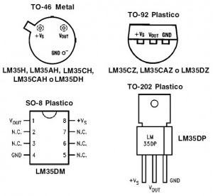
LM 35 temperature sensor IC is a IC chip production Natioanal Semiconductor which serves to determine the temperature of an object or space in the form of electric scale, or can also be defined as an electronic component that is used to change the temperature changes are accepted in the electrical wholesale changes. LM35 temperature sensor IC temperature change can change a change in voltage at the output. LM35 temperature sensor IC requires +5 volts DC source voltage and DC current consumption of 60 mA in operation. Physical form LM 35 temperature sensor is an IC chip with packaging that varies, in general packaging LM35 temperature sensor is packaged TO-92 as shown in the figure below.


Simple IC LM35 Temperature Sensor Characteristics


From the picture above it can be seen that the temperature sensor IC LM35 basically have 3 pin that serves as a source of supply voltage of +5 volts DC, as a result of sensing the output pin in the form of a change in the DC voltage and Vout pin to Ground.

IC LM35 temperature sensor characteristics are:

  •     Temperature sensitivity, with linear scaling factor between voltage and temperature 10 mVolt / º C, so it can be calibrated directly in centigrade.
  •     Have the accuracy or the accuracy of the calibration is 0.5 º C at 25 º C.
  •     Has a maximum operating temperature range between -55 º C to +150 º C. Working at a voltage of 4 to 30 volts.
  •     Has current low at less than 60 mA.
  •     Have a low self-heating (low-heating) of less than 0.1 º C in still air.
  •     Has a low output impedance is 0.1 W for 1 mA load.
  •     have Nonlinearities only about ± ¼ º C.

Read More..

Simple Up Controlled Negative Voltage Converter Circuit Diagram

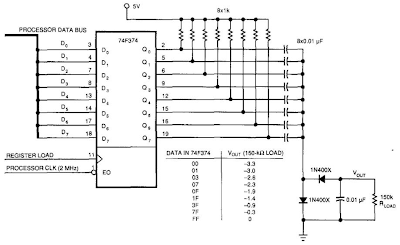
This Simple Up-Controlled Negative Voltage Converter Circuit Diagram was used to produce a variable negative voltage for contrast control of an LCD display. A 74F374 generates a square wave that is ac coupled to a rectifier and load. By using the uP clock and data from the processor bus, and properly timed load signal, the dc level generated can be controlled by the uP. 

Simple Up-Controlled Negative Voltage Converter Circuit Diagram 

Simple Up-Controlled Negative Voltage Converter Circuit Diagram
 
Read More..

Wednesday, December 18, 2013

Simple Frequency to Vvoltage Converter Circuit Diagram

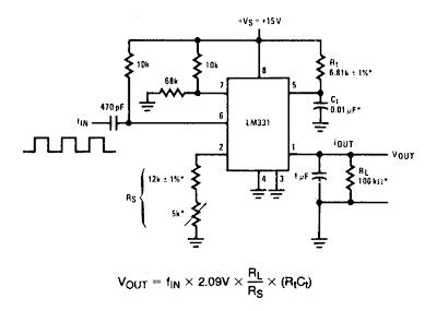
This is Simple Frequency to Vvoltage Converter Circuit Diagram. In these applications, a pulse input at % is differentiated by a C-R network and the negative-going edge at pin 6 causes the input comparator to trigger the timer circuit. Just as with a V-to-F converter, the average current flowing out of pin 1 is IaverAGE = i (1.1 RjC^ f. 

In this simple circuit, this current is filtered in the network RL = 100 k ohm and 1 µF. The ripple will be less than 10 mV peak, but the response will be slow, with a 0.1 second time constant, and settling of 0.7 second to 0.1%.


Simple Frequency to Vvoltage Converter Circuit Diagram

Simple Frequency to Vvoltage Converter Circuit Diagram


Simple Frequency to Vvoltage Converter Circuit Diagram
Read More..

Tuesday, December 17, 2013

How to Build a Simple Power supply Circuit Diagram

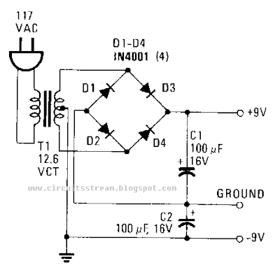
To day i share this post how to Build a simple power-supply circuit diagram lets start . This simple power supply circuit diagram delivers plus and minus 9 V to replace two 9-V batteries. The rectifier circuit is actually two separate full-wave rectifiers fed from the secondary of the transformer. One full-wave rectifier is composed of diodes D1 and D2, which develop +9 V, and the other is composed of D3 and D4, which develop -9 V. 

Each .diode from every pair rectifies 6.3 Vac, half the secondary voltage, and charges the associated filter capacitor to the peak value of the ac waveform, 6.3 x 1.414 ~ 8.9 V. Each diode should have a PIV, Peak Inverse `Voltage, rating that is at least twice the peak voltage from the transformer, 2 x 8.9 ~ 18 V. The 1N4001 has a PIV of 50 V. I hope you are enjoy this circuit.

Simple Power supply Circuit Diagram

Simple Power supply Circuit Diagram


Read More..

Wednesday, September 4, 2013

Simple But Reliable Car Battery Tester

This circuit uses the popular and easy to find LM3914 IC. This IC is very simple to drive, needs no voltage regulators (it has a built in voltage regulator) and can be powered from almost every source. This circuit is very easy to explain: When the test button is pressed, the Car battery voltage is feed into a high impedance voltage divider. His purpose is to divide 12V to 1,25V (or lower values to lower values).

This solution is better than letting the internal voltage regulator set the 12V sample voltage to be feed into the internal voltage divider simply because it cannot regulate 12V when the voltage drops lower (linear regulators only step down). Simply wiring with no adjust, the regulator provides stable 1,25V which is fed into the precision internal resistor cascade to generate sample voltages for the internal comparators. Anyway the default setting let you to measure voltages between 8 and 12V but you can measure even from 0V to 12V setting the offset trimmer to 0 (but i think that under 9 volt your car would not start).

 Car Battery Tester  Circuit diagram:


There is a smoothing capacitor (4700uF 16V) it is used to adsorb EMF noise produced from the ignition coil if you are measuring the battery during the engine working. Diesel engines would not need it, but Im not sure. If you like more a point graph rather than a bar graph simply disconnect pin 9 on the IC (MODE) from power. The calculations are simple (default)
For the first comparator the voltage is : 0,833 V corresponding to 8 V
* * * * * voltage is : 0,875 V corresponding to 8,4 V
for the last comparator the voltage is : 1,25 V corresponding to 12 V
Have fun, learn and dont let you car battery discharge... ;-)

author: Jonathan Filippi
e-mail: jonathan.filippi@virgilio.it
Read More..

Saturday, August 31, 2013

Simple Operational Amplifier DC Motor Driver

Using a simple operational amplifier and some other common electronic components can be designed a very simple DC motor driver that can be used for a 200mA motor application . Rb sets the bias point for transistors Q1 and Q2.

Because Vbe(ON) varies greatly with temperature, a guardband is required to prevent Q1 and Q2 from conducting simultaneously. RB should be selected such that the transistors do not conduct until lM equals the op amp quiescent supply current, Isy . The transistors will begin to conduct at about Vbe (on) = 0.5V. In this project :
RB= [vbe(on)/(lSY+ Im)]= 0.5/(0.0025 + 0.0025)=100 ohms

To maximize voltage swing across the motor, V1 must be minimized. If at full load V1 = 0.2V with V+ = 15V and VBE1 = 0.8V, the voltage across the motor will be:
VM = (V+ - 2) - VBE1 - V1 = (15 - 2) - 0.8 - 0.2 = 12.0V Vin may be scaled with a resistive divider as:
VIN= (R1 + R2)/R2 With R1 = 240k and R2 = 10k, VIN =5 volt lM = 200mA.
Read More..

Saturday, August 10, 2013

Simple 9V battery replacement circuit


This power supply circuit contains two charge-pump DC-DC converters which can delivery up to -10V for a 2,0V to 3,6V input voltage battery. For a current consumption of 7mA the output voltage it will drop to 9V, but this is enough to power a portable handheld instrument. The overall efficiency it will be up to 74% for a 2V input voltage and 60% for a 3.6V lithium polymer battery cell.

First charge-pump DC-DC converter based on MAX 619 from Maxim , C70851 smd code , delivers a regulated 5V +/- 4% output at max. 50mA. To maintain the greatest efficiency over the entire input voltage range, the MAX619s internal charge pump operates as a voltage doubler when input voltage ranges from 3.0V to 3.6V, and as a voltage tripler when it ranges from 2.0V to 2.5V.

The second charge pump converter use a TC682 circuit from Microchip and it provides an inverted doubled (-10V) output from a single positive supply (+5V regulated). An on-board 12kHz (typical) oscillator frequency provides the clock and only 3 external capacitors are required for full circuit implementation. Low output source impedance (typically 140Ω), provides output current up to 10mA.

10V DC-DC converter placement of circuit componentsComponents placement on printed circuit board
More voltage convertors:
    5V dc-dc converter this circuit can deliver over 1.6A at 5V and still work at 2.0V
    Max761 boost converter module from 5V to 13.5V or 12V, ideal for Flash Memory Programming
Read More..

Simple 0 30 Volts 2 5A Variable Power Supply Circuit Diagram

This is the Simple 0-30 Volts - 2-5A Variable Power Supply Circuit Diagram. This is a high quality power supply with a continuously variable stabilized output adjustable between 0 and 30VDC. the LM 723 is the heart of the power supply which drives the BD137 and then the 2N3055. The circuit provides short circuit protection. And has great stability at voltage changes. Drive the circuit with 24 Volts 3A from a transformer. the 2N3055 needs a good heat sink.

  0-30 Volts - 2-5A Variable Power Supply Circuit Diagram

 0-30 Volts - 2-5A Variable Power Supply Circuit Diagram
Read More..

Friday, August 9, 2013

Simple Noise limiter Circuit Diagram

This Noise limiter Circuit Diagram improves signal-to-noise ratio. It is connected between the detector output and the audio input (if high impedance) or at some relatively high-impedance section between two audio stages—preferably the low level stages.D1 and D2 can be any diode having relatively low forward resistance and very high back resistance. The circuit is excellent for receivers having bandwidths down to 2 or 3 kHz. Increase the value of Cl for receivers having narrower bandwidths . 

Noise limiter Circuit Diagram


Noise limiter Circuit Diagram

Read More..

Monday, August 5, 2013

Simple split power supply circuit Diagram

This circuit utilizes the quasi-complementary output stage of the popular LM380 audio power IC. The device is internally biased so that with no input the output is held midway between the supply rails Rl, which should be initially set to mid-travel, is used to nullify any inbalance in the output. 

Regulation of Vout depends upon the circuit feeding the LM380, but positive and negative outputs will track accurately irrespective of input regulation and unbalanced loads. 

The free-air dissipation is a little over 1 watt, and so extra cooling: may be required. The device is fully protected and will go into thermal shutdown if its rated dissipation is exceeded. Current limiting occurs if the output current exceeds 1 A. The input voltage should not exceed 20 V.

Simple split power supply circuit Diagram

Simple split power supply circuit Diagram

Read More..

Tuesday, July 30, 2013

Simple Current to voltage converter circuit Diagram

A filter removes the dc component of the rectified ac, which is then scaled to RMS

 Simple Current-to-voltage converter Circuit  Diagram


    Simple Current-to-voltage converter
Read More..

Monday, July 29, 2013

Simple Wide band 2 pole high pass filter

The Simple Wide band 2 pole high-pass filter circuit provides a 10MHz cutoff frequency. Resistor R3 ensures that the input capacitance of the amplifier does not interact with the filter response at the frequency of interest. An equivalent low pass filter is similarly obtained by capacitance and resistance transformation . 

Simple Wide band 2 pole high-pass filter Circuit Diagram

Simple Wide band 2 pole high-pass filter

Read More..

Friday, July 12, 2013

Simple 30 Watt VHF Amplifier by using 2SC1946A

The 30 watt amplifier schematic shown below provides an appropriate power boost with an input of 4 watt up to 6 watts. The circuit is designed to cover 88-108MHz FM Broadcast Band. However, the circuit is very stable at my place and provides a clean-output through seven (7) element Butter-worth low-pass filter.

Circuit Diagram:


Notes:
The heart of the circuit is 2SC1946A VHF RF power transistor. The transistor is specifically designed for operation in frequencies up to 175 MHz, with very good results. As you can see, the power line is well decoupled. The amplifier current can be over 5 amps. All the coils are made from 16gauge laminated wire (or Silver copper wire can do best) and the RFC can be of HF toroid core (as shown in the picture) or 6 holes ferrite bead.C3 and R1 forms snubber circuit while R2 and C6 prevent the amplifier from self-oscillation at VHF, sometimes you need to add 180 ohms in parallel with L7.That will cause the amplifier to dissipate UNDESIRABLE VHF thereby reducing spurious level.


The photo below is 60Watts VHF power amplifier using the above circuit. Two of 2SC1946A transistors are arranged at 90 degrees to each other and their outputs are combined using "Power Combiner Network”. It is quite difficult to combine powers at VHF and UHF bands.

However, I recommend that hobbies should stick to single power design due to its complicity and large rate of INTERFERENCE. (in attempt to go for double transistors which involves power combiner network). Since the two amplifiers are operating in different phase (out of phase).

Tuning:
Tuning of the amplifier is not hard at all. You just have to connect the output to a good antenna with a transmission line (RG214) of 50 ohms. First match the output network, and then do the same to the input network for a maximum power output. By way of adjustment, you can increase the output at its operating frequency.
Read More..

Thursday, July 4, 2013

Simple Mat Switch Circuit

This simple circuit produces a warning beep when somebody crosses a protected area in your home or office. The switch, hidden be-low the floor mat, triggers the alarm when the person walks over it.

The circuit uses a conductive foam as the switch. It can be two small pieces of conductive pads usually used to pack sensitive ICs as antistatic cover. Alternatively, you can make the switch by coating conducting carbon ink on two small pieces of a copper-clad board.

Circuit diagram :

Link


Simple Mat Switch Circuit Diagram

When the circuit is in standby mode, transistor T1 does not conduct, since its base is floating. When the person walks, the switch is pressed and current flows through R1 and the switch to provide positive bias to transistor T1. Transistor T1 conducts and its collector voltage drops, which acts as a negative trigger input for the monostable wired around IC NE555 (IC1).

IC1 outputs a pulse of fifty-seconds duration with preset values of R4 and C3. This pulse is applied to the buzzer through transistor T2. The buzzer sounds a warning beep on unauthorised entry. The pulse duration can be changed to the desired value by changing the values of R4 and C3. Resistor R2 in the circuit makes the trigger pin of IC1 high to prevent false triggering.

Assemble the circuit on a general-purpose PCB and enclose in a plastic case. Use a 9V battery to power the circuit. Connect the touchpad switch with the PCB and hide under the mat at the entrance. The PCB can be mounted on the nearby wall.

Make the switch carefully using conducting foam or copper clad coated with conducting ink. Place the two pieces with their conducting surface facing each other. Solder carefully a thin copper electric wire and ensure that it makes contact when the two plates touch together on pressing. Provide two 1cm rubber tabs between the plates to avoid touch in the standby mode.


http://streampowers.blogspot.com/2012/06/simple-mat-switch-circuit.html 
Read More..

Tuesday, May 14, 2013

Simple IF Signal Generator

http://www.electronic-circuits-diagrams.com/generatorsimages/1.gifHere is a versatile circuit of IF signal generator which may be of interest to radio hobbyists and professionals alike.Transistors T1 and T2 form an astable multivibrator oscillating in the audio frequency range of 1 to 2 kHz
Read More..

Wednesday, April 10, 2013

Simple Steam Whistle

This circuit consists of six square wave oscillators. Square waves are made up of a large number of harmonics. If six square waves with different frequencies are added together, the result will be a signal with a very large number of frequencies. When you listen to the result you’ll find that it is very similar to a steam whistle. The circuit should be useful in modelling or even in a sound studio.
Circuit diagram :
Simple Steam Whistle-Circuit Diagram
Simple Steam Whistle Circuit Diagram

This circuit uses only two ICs. The first IC, a 40106, contains six Schmitt triggers, which are all configured as oscillators. Different frequencies are generated by the use of different feedback resistors. The output signals from the Schmitt triggers are mixed via resistors. The resulting signal is amplified by IC2, an LM386. This IC can deliver about 1 W of audio power, which should be sufficient for most applications. If you leave out R13 and all components after P1, the output can then be connected to a more powerful amplifier. In this way a truly deafening steam whistle can be created. The ‘frequency’ of the signal can be adjusted with P2, and P1 controls the volume.


Streampowers
Read More..