Sunday, December 22, 2013

Simple Security Door Electronic Key

It is a relatively simple circuit of electronic lock of safety with code of 7 digits. It should is given attention in the time that will be stepped the keys, that shape code and it does not exist it delays. With the right step of keys and if code is right then is activated exit Q7 for roughly 4 seconds, driving the transistor Q2, which with the line can drive one relay, for the opening of door, or any other circuit.

Security Door Electronic Key Circuit diagram :

security-door-electronic-key Circuit diagram

With LED D we can have optical clue of activation. The code of circuit, as it has been given have been:1704570 but can change, if we change the connections between in the exits of IC1 and the switches.

Parts List :
  • R1-7=4.7Kohm
  • R8=15Kohm
  • R9=1Mohm
  • R10-13=10Kohm
  • R11=100ohm
  • R12=220Kohm
  • R14=1.2Kohm
  • C1-3=100nF 100V
  • C2=4.7uF 25V
  • D1-2=1N4148
  • D3=RED LED 3mm
  • IC1=4022
  • Q1=BS170
  • Q2=BD679
  • S1-10=Push button or keyboard
Source : http://www.ecircuitslab.com/2012/08/security-door-electronic-key.html
Read More..

Pushbutton Switch

This circuit acts like a two-position switch but is operated using a pushbutton. After power has been applied, the circuit is in the following initial state: the bases of T1 and T2 are at the positive supply potential and the base of T3 is at ground potential. All transistors are cut off. The other contact of the pushbutton is at ground potential. No current flows through the relay coil and the status LED is off.

Pushbutton Switch Circuit diagram :
Pushbutton Switch-Circuit-diagram

If the pushbutton is pressed, T2 and (after a slight delay due the RC network) T3 switch on. The collector of T3 is now nearly at ground potential, so current flows through the relay coil and the function LED is illuminated. T1 can also switch on. This situation is stable, since ground potential can reach the base of T2 via R1, so nothing changes when the pushbutton is released. C1 is charged via R3 to cause a positive potential to be present at the pushbutton. If the pushbutton is now pressed again, it connects a positive potential to the base of T2 instead of the ground potential. This causes everything to toggle back into the initial state.

Similar operation can be obtained using a thyristor circuit, and in fact T2 and T3 form a sort of thyristor. However, the circuit shown here is largely independent of the voltage and current demands of the connected load. The relay coil should be suit-able for the supply voltage (5–12 V) and should not draw more than 250 mA, since otherwise T3 will go up in smoke. With our lab prototype, we measured a current consumption of 70 mA in the ‘on’ state and less than 0.1 mA in the ‘off’ state.

Source : www.ecircuitslab.com
Read More..

Saturday, December 21, 2013

Automatic Battery Charger

Normally, chargers available in the market do not have any sort of control except for a ro-tary switch that can select different tap-pings on a rheostat, to vary the charging current. This type of control is not adequate because of the irregular fluctuations in the mains supply, rendering the control ineffective.  A simple circuit intended for automatic charging of lead-acid batteries is presented here. It is flexible enough to be used for large capacity inverter batteries. Only the rating of transformer and power transistor needs to be increased.

Automatic Battery Charger Circuit Diagram

Automatic Battery Charger Circuit Diagram

The circuit has been basically designed for a car battery (about 40 Ah rating), which could be used for lighting two 40W tube lights. The circuit includes Schmitt trigger relay driver,float charger,and battery voltage monitor sections.  The Schmitt trigger is incorporated to avoid relay chattering. It is designed for a window of about 1V. During charging, when the battery voltage increases be-yond 13.64V, the relay cuts off and the float charging section continues to work. When battery voltage goes below 11.66V, the relay is turned on and direct (fast) charging of the battery takes place at around 3A.  In the Schmitt trigger circuit, resistors R1 and R2 are used as a simple voltage divider (divide-by-2) to provide battery voltage sample to the inverting input terminal of IC1. The non-invert-ing input terminal of IC1 is used for reference input derived from the output of IC2 (7806), using the potentiometer arrangement of resistors R3 (18 kilo-ohm) and R4 (1 kilo-ohm).

LED1 is connected across relay to indicate fast charging mode. Diodes D3 and D6 in the common leads of IC2 and IC3 respectively provide added protecion to the regulators.  The float charging section, comprising regulator 7812, transistors T3 and T4, and few other discrete components, becomes active when the battery volt-age goes above 13.64V (such that the relay RL1 is deenergised). In the energised state of the relay, the emitter and collector of transistor T4 remain shorted, and hence the float charger is ineffective and direct charging of battery takes place.

The reference terminal of regulator (IC3) is kept at 3.9V using LED2, LED3, and diode D6 in the common lead of IC3 to obtain the required regulated output (15.9V), in excess of its rated output, which is needed for proper operation of the circuit. This output voltage is fed to the base of transistor T3 (BC548), which along with transistor T4 (2N3055) forms a Darlington pair. You get 14.5V output at the emitter of transistor T4, but because of a drop in diode D7 you effectively get 13.8V at the positive terminal of the battery. When Schmitt trigger switches ‘on’ relay RL1, charging is at high current rate (boost mode). The fast charging path, starting from transformer X2, comprises diode D5, N/O contacts of relay RL1, and diode D7.

The circuit built around IC4 and IC5 is the voltage monitoring section that provides visual display of battery voltage level in bar graph like fashion. Regulator 7805 is used for generating reference voltage. Preset VR1 (20 kilo-ohm) can be used to adjust voltage levels as indicated in the circuit. Here also a pot meter arrangement using resistors R7, R8, and R9 is used as ‘divide by 3’ circuit to sample the battery voltage. When voltage is below 10V, the buzzer sounds to indicate that the safe dis-charge limit has been exceeded.

Source: http://www.ecircuitslab.com/2011/11/normally-chargers-available-in-market.html


Read More..

Simple IC LM35 Temperature Sensor Characteristics

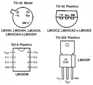
LM 35 temperature sensor IC is a IC chip production Natioanal Semiconductor which serves to determine the temperature of an object or space in the form of electric scale, or can also be defined as an electronic component that is used to change the temperature changes are accepted in the electrical wholesale changes. LM35 temperature sensor IC temperature change can change a change in voltage at the output. LM35 temperature sensor IC requires +5 volts DC source voltage and DC current consumption of 60 mA in operation. Physical form LM 35 temperature sensor is an IC chip with packaging that varies, in general packaging LM35 temperature sensor is packaged TO-92 as shown in the figure below.


Simple IC LM35 Temperature Sensor Characteristics


From the picture above it can be seen that the temperature sensor IC LM35 basically have 3 pin that serves as a source of supply voltage of +5 volts DC, as a result of sensing the output pin in the form of a change in the DC voltage and Vout pin to Ground.

IC LM35 temperature sensor characteristics are:

  •     Temperature sensitivity, with linear scaling factor between voltage and temperature 10 mVolt / º C, so it can be calibrated directly in centigrade.
  •     Have the accuracy or the accuracy of the calibration is 0.5 º C at 25 º C.
  •     Has a maximum operating temperature range between -55 º C to +150 º C. Working at a voltage of 4 to 30 volts.
  •     Has current low at less than 60 mA.
  •     Have a low self-heating (low-heating) of less than 0.1 º C in still air.
  •     Has a low output impedance is 0.1 W for 1 mA load.
  •     have Nonlinearities only about ± ¼ º C.

Read More..

Does not exist to bandwidth restrictions and limits the number of users

It is also the alternative solution for perfect cell phone jammer .
Operation of mobile TV technology. Core technology. For mobile TV technology, the very early abroad have begun to research. Japan in 1999 by a terrestrial broadcast digital television standard ISDB-T in Europe in 2002 began to study this standard, and in February 2004 by the DVB-H standard. South Korea in February 2003, clearly stated, "Digital Multimedia Broadcasting", and support standard named DMB, The country of Chinas mobile TV standard be introduced before the end of 2006. In October, the State Administration of Radio, Film and Television issued recommended standards: of STiMi technical standards. The formulation of these standards, to provide a basis for the development of mobile TV. It is for the supplementary installation method of perfect cell phone jammer on the outer wall.
At present, the core technology of mobile TV, is the network operator implementation. These technologies or standards, mainly in three ways: two-way communication that can use the mobile network, to provide users with personalized service; convenient right to business monitoring, management, accounting and control; do not change the phone hardware platform network bandwidth is limited, and could easily lead customers to compete for resources; low image resolution, image quality is affected by the impact of network bandwidth. Ground-based radio and television technology. Basically completed ready for commercialization. Does not exist to bandwidth restrictions and limits the number of users, high image quality; low sensitivity to the user, the capacity of the unexpected and emergency events. Usually there is no uplink, it is difficult to achieve the users personalized service. Adjust the distance between positions of installing perfect cell phone jammer .
Difficult to identify, control, interaction, billing and positioning services; terminal a digital television receiver unit must be increased. Have been commercialized for one year the use of satellites for mobile video broadcasting services more efficient; the satellites wide coverage. Personalized and interactive subject to certain constraints; terminal circuit module must be increased to be able to receive satellite TV signals. Based on the mobile communication network. In this way is actually through the mobile communication network using streaming media technology to achieve mobile TV program delivery, as well as the user on demand. The United States and Chinas mobile operators launched mobile TV services rely on the existing mobile network. Perfect cell phone jammer is hung inside the plant.
Read More..

Simple Up Controlled Negative Voltage Converter Circuit Diagram

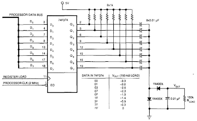
This Simple Up-Controlled Negative Voltage Converter Circuit Diagram was used to produce a variable negative voltage for contrast control of an LCD display. A 74F374 generates a square wave that is ac coupled to a rectifier and load. By using the uP clock and data from the processor bus, and properly timed load signal, the dc level generated can be controlled by the uP. 

Simple Up-Controlled Negative Voltage Converter Circuit Diagram 

Simple Up-Controlled Negative Voltage Converter Circuit Diagram
 
Read More..

The paste component can greatly enhance the performance of cell phone jammer

cell phone jammer will not interfere with any other electronic equipment.
Re-emphasized the quality of service at the same time, consumers also requires improvements in the environment, price, equipment, technology, quality of employees. In addition, the very credibility

of the optical shop. We must take seriously the views and suggestions of consumers, and these should be our course of action, we have to fight for the hearts of consumers, to gain their trust,

which is what we beat the opponent, occupied the great secret of the market. According to the survey results and analysis for the present market situation, the following suggestions and strategies.

Make sure that the quality of service to establish a good reputation. Consumers the choice of the optical shop, first focus on the credibility of the optical shop. In the locations where the using

of the cell phone is needed to be forbidden and the cell phone signal is needed to be shielded, cell phone jammer is needed.
Therefore, for this consumer group, it is recommended to strengthen the Companys internal services and quality of construction, increase advertising efforts (in addition to traditional mass media

of television, newspapers and radio, network, should increase, such as bookstores, Square public and cultural places of propaganda), the same time, establish a good reputation and image. Positive

publicity to tap the potential market. The consumer group, will tend to glasses to hold a kind of hesitation, wait and see, and even negative attitude. Therefore, for this phenomenon, it is

recommended that through effective propaganda, dispel the doubts of the minds of consumers, to encourage consumers to wear glasses. This regard, can be reflected in the service process. The paste

component can greatly enhance the performance of cell phone jammer .The material of cell phone jammer requires highly
In the service of process to be clear, serious eye health knowledge to explain to the consumer, inform glasses maintenance of knowledge, and described in detail the characteristics of a variety of

lenses, to inform consumers of myopia without the adverse effects of glasses, more important is the strict audit procedures of the glasses. Also recommended the establishment of "post-consumer

glasses eyes health status tracking system" more humane, more user-friendly service. At the same time, to carry out social advocacy, public service and other activities are also to be considered.

Establish a wide range of well-known brand image. The perfect parameter and high performance of cell phone jammer can be guaranteed.
Read More..