Showing posts with label using. Show all posts

Wednesday, September 4, 2013

High Temperature Detector Using UM3561

This heat detector alarm electronic project is designed using the UM3561 sound generator circuit and some other common electronic parts . This heat detector circuit project uses a complementary pair comprising npn and pnp transistor to detect heat . T3 and T4 transistors connected in darlington configuration are used to amplify the audio signal from the UM3561 ic .

High Temperature Detector Circuit Diagram


When the temperature close to the T1 transistor is hot , the resistance to the emitter –collector goes low and it starts conducting . In same time T2 transistor conducts , because its base is connected to the collector of T1 transistor and the RL1 relay energized and switches on the siren which produce a fire engine alarm sound .
The relay used in this project must be a 6 volt / 100 ohms relay and the speaker must have a 8 ohms load and 1 watt power . This electronic project must be powered from a 6 volts DC, but the UM3561 IC is powered using a 3 volt zener diode , because the alarm sound require a 3 volts dc power supply .
Read More..

Tuesday, September 3, 2013

Stereo Headphone Amplifier Using LM4882

Using the LM48824 integrated circuit , can be designed a very simple stereo headphone amplifier for portable devices .

Stereo Headphone Amplifier Circuit diagram

The LM48824’s Stereo Headphone Amplifier (Class G architecture ) increases audio (MP3, mobile TV, etc.) playback time with its adaptive power supply approach that enables very low supply rails, which doubles the power-efficiency compared to typical Class AB headphone amplifiers.

A high output impedance mode allows the LM48824s outputs to be driven by an external source without degrading the signal.
Read More..

Monday, September 2, 2013

DC Servo Motor Circuit Using A3952S

A3952S motor driver is capable of continuous output currents up to 2 A and has an operating voltages range up to 50 V. Warning , the 50 operating voltage is to power the motor , for the logic controller you will need a 5 volts Dc power supply .

DC Servo Motor Circuit  Diagram

This simple DC servo motor circuit design that can be used in various electronic projects . As you can see in the circuit schematic this Dc servo motor driver schematic circuit use just one integrated circuit and other few external electronic components .

With bidirectional dc servo motors, the PHASE terminal can be used for mechanical direction control. Similar to when braking the motor dynamically, abrupt changes in the direction of a rotating motor produce a current generated by the back EMF. The current generated will depend on the mode of operation.
Read More..

Sunday, September 1, 2013

AM Radio Receiver Using by TEA5551T

Using TEA5551T monolithic integrated radio circuit can be designed a AM radio receiver circuit which is designed for use as a portable radio receiver with headphones . 

AM Radio Receiver Circuit diagram

The TEA5551T radio receiver circuit contains all is needed for a AM radio receiver circuit (a complete AM part and dual AF amplifier with low quiescent current).The TEA5551T support a input voltage range (VS) from 1.8 V to 4.5 V but the typical voltage is 3 volts .Because in most case we don’t find to buy inductors you need to build the inductors L1 , L2 , L3 . In the picture bellow you can see the construction data for these three inductors .
Read More..

Saturday, August 31, 2013

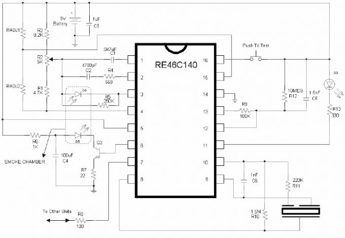
Smoke Detector Alarm Using RE46C140

Using the RE46C140 circuit can be designed a very simple smoke detector alarm using few external electronic components . The RE46C140 IC is a low power CMOS photoelectric type smoke detector IC that will provide all the required features for a photoelectric type smoke detector project . This smoke detector alarm design incorporates a gain selectable photo amplifier for use with an infrared emitter detector pair. An internal oscillator strobes power to the smoke detection circuitry for 100us every 10 seconds to keep standby current to a minimum. If smoke is sensed the detection rate is increased to verify an alarm condition.

Smoke Detector Alarm Circuit Diagram


An interconnect pin allows multiple detectors to be connected such that when one units alarms, all units will sound. In standby the LED is pulsed on for 10mS every 43 seconds . In a local alarm condition or the push to test alarm the LED pulse frequency is increased to once every 5 seconds. In the case of a remote alarm the LED not active. In the timer mode of operation the LED is pulsed on for 10mS every 10 seconds.

A comparator compares the photo amp output to an internal reference voltage. If the required number of consecutive smoke conditions is met the device will go into local alarm and the horn will be active. The bidirectional IO pin allows interconnection of multiple detectors. In a local alarm condition this pin is driven high immediately through a constant current source. Shorting this output to ground will not cause excessive current. The IO is ignored as an input during a local alarm. This smoke detector circuit must be powered from a 9 volt DC power supply .
Read More..

Sunday, August 11, 2013

Mobile Charger using Bike Battery


When a surge voltage exceeding maximum voltage rating of the regulator is applied to the input or when a voltage in excess of the input voltage is applied to the output, the regulator will be destroyed. If the input terminal shorts with the ground, the output voltage increases above the input voltage(ground potential)and the charge in the capacitor connected to the output flows into the input side which is also fatal to the regulator.

Both these situations can be avoided by using the Zener at the input and the diode D1 across the regulator. Capacitor C1 and C2 provide stability to the regulator and these should be soldered close to the legs of the regulator. Capacitor C3 act as a buffer to give constant voltage in the output.
7805 IC can tolerate maximum 35 volts and its current rating is 1 Amps maximum. Resistor R1 restricts the charging current to around 330 mA as per the Ohms law.

Even if the current is low, charging process will not be affected. Slow charging with 80 to 100 mA current is generally advised. But in case of an emergency, quick charging can be done with high current Assemble the circuit on a Perf board and enclose in a small case that can be fitted near the Bike battery. Use suitable pins to connect with the Mobile phone. Charging current can be tapped from the battery using Alligator Clips. Before using the circuit, double check the connections especially the polarity of connectors and measure output voltage and current using a Digital Multi Meter. The same circuit can be used for charging Mobile battery from 12 volt Car battery or from a 12 volt Solar panel.
Read More..

Friday, August 9, 2013

Heat Detector Alarm using UM3561

A very simple heat detector alarm electronic project can be designed using the UM3561 sound generator circuit and some other common electronic parts . This heat detector electronic circuit project uses a complementary pair comprising npn and pnp transistor to detect heat Collector of T1 transistor is connected to the base of the T2 transistor , while the collector of T2 transistor is connected to RL1 relay T3 and T4 transistors connected in darlington configuration are used to amplify the audio signal from the UM3561 ic.

Circuit Project: Heat detector alarm circuit using UM3561
When the temperature close to the T1 transistor is hot , the resistance to the emitter –collector goes low and it starts conducting . In same time T2 transistor conducts , because its base is connected to the collector of T1 transistor and the RL1 relay energized and switches on the siren which produce a fire engine alarm sound. This electronic circuit project must be powered from a 6 volts DC power supply , but the UM3561 IC is powered using a 3 volt zener diode , because the alarm sound require a 3 volts dc power supply. The relay used in this project must be a 6 volt / 100 ohms relay and the speaker must have a 8 ohms load and 1 watt power.
 
 
Streampowers
Read More..

Tuesday, July 30, 2013

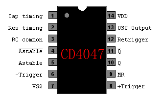
12VDC – 220VAC Inverter Using Cmos CD4047

12VDC – 220VAC Inverter Using Cmos CD4047
This circuit inverter converts 12V DC battery to AC 22oV as the replacement of home energy. The inverter can be used for small electronic devices such as lamps, radio, phone charger, disc player, etc.
12VDC – 220VAC Inverter Using Cmos CD4047
The inverter circuit is a central component, the CMOS 4047, and converts a DC voltage of 12 V to 220 V AC voltage. 4047 is used as an astable multivibrator. The pin 10 and 11 we find a symmetrical rectangular signal is amplified by Darlington transistors T1 and T2 trailer, and finally reaches the secondary coil of a transformer of the network (2 x 10V/100VA). Primary coil voltage is 220 AC voltage terminals. For best performance, use a toroidal core transformer with low losses. P1 to the output frequency can be regulated within certain limits (50 ... 400 Hz).
Read More..

Friday, July 12, 2013

Simple 30 Watt VHF Amplifier by using 2SC1946A

The 30 watt amplifier schematic shown below provides an appropriate power boost with an input of 4 watt up to 6 watts. The circuit is designed to cover 88-108MHz FM Broadcast Band. However, the circuit is very stable at my place and provides a clean-output through seven (7) element Butter-worth low-pass filter.

Circuit Diagram:


Notes:
The heart of the circuit is 2SC1946A VHF RF power transistor. The transistor is specifically designed for operation in frequencies up to 175 MHz, with very good results. As you can see, the power line is well decoupled. The amplifier current can be over 5 amps. All the coils are made from 16gauge laminated wire (or Silver copper wire can do best) and the RFC can be of HF toroid core (as shown in the picture) or 6 holes ferrite bead.C3 and R1 forms snubber circuit while R2 and C6 prevent the amplifier from self-oscillation at VHF, sometimes you need to add 180 ohms in parallel with L7.That will cause the amplifier to dissipate UNDESIRABLE VHF thereby reducing spurious level.


The photo below is 60Watts VHF power amplifier using the above circuit. Two of 2SC1946A transistors are arranged at 90 degrees to each other and their outputs are combined using "Power Combiner Network”. It is quite difficult to combine powers at VHF and UHF bands.

However, I recommend that hobbies should stick to single power design due to its complicity and large rate of INTERFERENCE. (in attempt to go for double transistors which involves power combiner network). Since the two amplifiers are operating in different phase (out of phase).

Tuning:
Tuning of the amplifier is not hard at all. You just have to connect the output to a good antenna with a transmission line (RG214) of 50 ohms. First match the output network, and then do the same to the input network for a maximum power output. By way of adjustment, you can increase the output at its operating frequency.
Read More..

Thursday, July 11, 2013

Heat Detector Alarm Using the UM3561

A very simple heat detector alarm electronic project can be designed using the UM3561 sound generator circuit and some other common electronic parts . This heat detector electronic circuit project uses a complementary pair comprising npn and pnp transistor to detect heat . Collector of T1 transistor is connected to the base of the T2 transistor , while the collector of T2 transistor is connected to RL1 relay . T3 and T4 transistors connected in darlington configuration are used to amplify the audio signal from the UM3561 ic .

Heat Detector Alarm Circuit diagram


When the temperature close to the T1 transistor is hot , the resistance to the emitter –collector goes low and it starts conducting . In same time T2 transistor conducts , because its base is connected to the collector of T1 transistor and the RL1 relay energized and switches on the siren which produce a fire engine alarm sound . This electronic circuit project must be powered from a 6 volts DC power supply , but the UM3561 IC is powered using a 3 volt zener diode , because the alarm sound require a 3 volts dc power supply . The relay used in this project must be a 6 volt / 100 ohms relay and the speaker must have a 8 ohms load and 1 watt power .
Read More..

Tuesday, July 9, 2013

50W Power Amplifier Using STK084

This is the circuit diagram of 50W power amplifier circuit which built based on single power amplifier chip of STK084. Its an well-known old IC for audio frequency (AF) amplifier.

50W Power Amplifier Circuit Diagram

This circuit requires dual polarity / split power supply with maximum supply of ± 50. The recommended supply is ± 35 / 2-3A DC current. You may use this split power supply circuit for the amplifier. Use 28V center tap transformer to get about ± 36V output.

Technical Details:

Power output: 50W
RL : 8 Ohm
TDH : 0.2 %
Rin : 52K
Gain : 26.4 dB
Noise : 0.3 mV

Take a note that heatsink is required to be mounted on the power IC since it will going to hot when operated and deliver high power output (high audio volume level).
Read More..

CMOS Toggle Flip Flop Using Push Button

The circuit below uses a CMOS dual D flip flop (CD4013) to toggle a relay or other load with a momentary push button. Several push buttons can be wired in parallel to control the relay from multiple locations.A high level from the push button is coupled to the set line through a small (0.1uF) capacitor. The high level from the Q output is inverted by the upper transistor and supplies a low reset level to the reset line for about 400 mS, after which time the reset line returns to a high state and resets the flip flop. The lower flip flop section is configured for toggle operation and changes state on the rising edge of the clock line or at the same time as the upper flip flop moves to the set condition. The switch is debounced due to the short duration of the set signal relative to the long duration before the circuit is reset.

CMOS Toggle Flip Flop Using Push Button Circuit Diagram


CMOS Toggle Flip Flop Using Push Button

 The Q or Qbar outputs will only supply about 2 mA of current, so a buffer transistor or power MOSFET is needed to drive a relay coil, or lamp, or other load. A 2N3904 or most any small signal NPN transistor can be used for relay coil resistances of 250 ohms or more. A 2N3053 or medium power (500 mA) transistor should be used for coil resistances below 250 ohms. The 47 ohm resistor and 10uF capacitor serve to decouple the circuit from the power supply and filter out any short duration noise signals that may be present. The RC network (.1/47K) at the SET line (pin 8) serves as a power-on reset to ensure the relay is denergized when circuit power is first applied. The reset idea was suggested by Terry Pinnell who used the circuit to control a shed light from multiple locations.
Read More..

Friday, July 5, 2013

Constructing a Universal Power Supply using LM317 Rise

This is a basic,  Universal Power Supply voltage regulator circuit using an LM317, 3-terminal regulator in a TO-220package. The Universal Power Supply output voltage can be set to anywhere in the range one.5V to 30V by selecting resistances. By using a potentiometer, R2, as of the resistors you can dial up the output voltage wanted. Either AC or DC input can be supplied to the PCB by a socket or terminal block. Connection can be either way around. This is because they have provided a bridge rectifier on board. The input DC voltage to the regulator must be at least two.5V above the necessary output voltage. An off/on switch is provided.

For lots of applications (say 12V at 60mA) a heat sink wont be required. The LM317 will provide slightly higher output voltages than 30 volts. However, for most hobbyists over 30V wont be needed. So to make a small PCB they have used some electrolytic capacitors rated to 35 volts. To be safe for continuous operation the maximum input DC voltage to the regulator ought to not be over 33V. With a two.5V to three.0V drop across the regulator this will give a regulated output of 30V. You can draw up to one.5A from the LM317. In case you need higher then use an LM338T rated to 5A.

When outside capacitors are used with any IC regulator it is lovely practice to add protection diodes to prevent the capacitors discharging back in to the regulator in the event of abnormal operating conditions, like a sudden short circuit on the input or the output, or a back emf from an inductive load. That is the function of D one and D Two.

The worth of R1 can range anywhere from 120R to 1200R However, circuits from most other sources settle on using either 220R or 250R. They have used 240R or 250R. The voltage drop across R1is one.25V for all values, and this is the key to the design. one.25V is the reference voltage of the regulator. Whatever current flows through R1 also flows through R2, and the sum of the voltage drops across R1 and R2 is the output voltage. (Additional current Id also flows in R2 but it is usually 50uA so is negligible.)

The design formula are:
VOUT = 1.25 (1 + R2/R1) volts, or alternatively
R2/R1 = (VOUT/1.25) - 1

So in case you know VOUT & R1 is 250R then you can calculate R2. In case you find that the 5K potentiometer used forR2 does not give you the degree of fine control over the voltage output range that you need then you can use these formula to fine-tune R1 & R2 to better suited values.


Universal Power Supply Schematic Diagram


Read More..

Wednesday, June 12, 2013

3 Wire Serial LCD Circuits using a Shift Register


74HC595 is a high-speed 8-bit serial in, serial or parallel-out shift register with a storage register and 3-state outputs.
The shift register and storage registers have separate clocks, SH_CP and ST_CP respectively. Data in the shift register is shifted on the positive-going transitions of SH_CP, and the content of shift register will be transferred to the storage register on a positive-going transition of the ST_CP. If we tie both the clocks together, the shift register will always be one clock ahead of the storage register. The 8-bit data of the storage register will appear at the parallel output (Q0-Q7) when the output enable (OE) is low.
In this project, SH_CP and ST_CP are tied together. So, if we want to receive a serially transferred 8-bit into parallel form at Q0-Q7, an extra clock pulse is required after transmitting the 8-th bit of serial data because the clocks are tied and the storage register is 1-clock behind the shift register. 

HD44780-based character LCD

 
 All HD44780 based character LCD displays are connected using 14 wires: 8 data lines (D0-D7), 3 control lines (RS, E, R/W), and three power lines (Vdd, Vss, Vee). Some LCDs may have LED backlight and so they may have additional connections (usually two: LED+ and LED-).

Providing detail explanation of individual LCD pin doesnt fall within the scope of this project. If you are a beginner with LCD, I recommend to read these two articles first from Everyday Practical Electronics magazine : How to use intelligent LCDs  

 The SH_CP (11) and ST_CP (12) clock inputs of 75HC595 are tied together, and will be driven by one microcontroller pin. Serial data from microcontroller is fed to the shift register through DS (14) pin. OE (13) pin is grounded and reset pin MR (10) is pulled high. Parallel outputs Q0-Q3 from 74HC595 are connected to D4-D7 pins of the LCD module. Similarly, Q4 output serves for RS control pin. If the LCD module comes with a built-in backlight LED, it can simply be turned ON or OFF through LED control pin shown above. Pulling the LED pin to logic high will turn the back light ON.

 Software 
A first, a bit of data fed to DS pin of 74HC595 appears at Q0 output after 2 clocks (because SH_CP and ST_CP are tied). So, sending 4-bit data (D4-D7) and an RS signal require 6 clock pulses till they appear at Q0-Q4 outputs respectively. When the LCD module is turned ON, it is initialized in 8-bit mode. A number of initializing commands should be sent to operate the LCD module in 4-bit mode. All the driver routines that are discussed here are written in mikroC compiler. They work only for a 16x2 LCD module. User can modify the initialization operations inside the Initialize_LCD() routine to account for other LCD configurations. The driver routines and their functions are described below. 
- Initialize_LCD() : It initializes the LCD module to operate into 4-bit mode, 2 lines display, 5x7 size character, display ON, and no cursor.
- Write_LCD_Data() : Sends a character byte to display at current cursor position. 
- Write_LCD_Cmd() : Write a command byte to the LCD module. 
- Write_LCD_Nibble() : Data or command byte is sent to the LCD module as two nibbles. So this function routine takes care for sending the nibble data to the LCD module.
- Write_LCD_Text() : This routine is for sending a character string to display at current cursor position.
- Position_LCD() : To change the current cursor position
At the beginning of your program, you need to define Data_Pin, Clk_Pin, and Enable_Pin to the chosen microcontroller ports. I am going to demonstrate here how to use these driver routines to display two blinking character strings, Message1 and Message2, at different locations. I am going to test our serial LCD module with PIC12F683 microcontroller. The test circuit is shown below.
Note: My PIC12F683 Settings
Running at 4 MHz internal clock, MCLR disabled, WDT OFF.
Clock, Data, and Enable lines are served through GP1, GP5, and GP2 ports.


/* 3-wire Serial LCD using 74HC595
Rajendra Bhatt, Sep 6, 2010
*/
 
sbit Data_Pin at GP5_bit;
sbit Clk_Pin at GP1_bit;
sbit Enable_Pin at GP2_bit;
 
// Always mention this definition statement
unsigned short Low_Nibble, High_Nibble, p, q,  Mask, N,t, RS, Flag, temp;
 
void Delay_50ms(){
 Delay_ms(50);
}
 
void Write_LCD_Nibble(unsigned short N){
 Enable_Pin = 0;
 // ****** Write RS *********
 Clk_Pin = 0;
 Data_Pin = RS;
 Clk_Pin = 1;
 Clk_Pin = 0;
 // ****** End RS Write
 
 // Shift in 4 bits
 Mask = 8;
  for (t=0; t<4; t++){
   Flag = N & Mask;
   if(Flag==0) Data_Pin = 0;
   else Data_Pin = 1;
   Clk_Pin = 1;
   Clk_Pin = 0;
   Mask = Mask >> 1;
  }
  // One more clock because SC and ST clks are tied
  Clk_Pin = 1;
  Clk_Pin = 0;
  Data_Pin = 0;
  Enable_Pin = 1;
  Enable_Pin = 0;
}
// ******* Write Nibble Ends
 
 void Write_LCD_Data(unsigned short D){
 RS = 1; // It is Data, not command
 Low_Nibble = D & 15;
 High_Nibble = D/16;
 Write_LCD_Nibble(High_Nibble);
 Write_LCD_Nibble(Low_Nibble);
 }
 
void Write_LCD_Cmd(unsigned short C){
 RS = 0; // It is command, not data
 Low_Nibble = C & 15;
 High_Nibble = C/16;
 Write_LCD_Nibble(High_Nibble);
 Write_LCD_Nibble(Low_Nibble);
}
 
void Initialize_LCD(){
 Delay_50ms();
 Write_LCD_Cmd(0x20); // Wake-Up Sequence
 Delay_50ms();
 Write_LCD_Cmd(0x20);
 Delay_50ms();
 Write_LCD_Cmd(0x20);
 Delay_50ms();
 Write_LCD_Cmd(0x28); // 4-bits, 2 lines, 5x7 font
 Delay_50ms();
 Write_LCD_Cmd(0x0C); // Display ON, No cursors
 Delay_50ms();
 Write_LCD_Cmd(0x06); // Entry mode- Auto-increment, No Display shifting
 Delay_50ms();
 Write_LCD_Cmd(0x01);
 Delay_50ms();
}
 
void Position_LCD(unsigned short x, unsigned short y){
 temp = 127 + y;
 if (x == 2) temp = temp + 64;
 Write_LCD_Cmd(temp);
}
 
void Write_LCD_Text(char *StrData){
 q = strlen(StrData);
 for (p = 0; p
  temp = StrData[p];
  Write_LCD_Data(temp);
 }
 
}
 
char Message1[] = "3-Wire LCD";
char Message2[] = "using 74HC595";
 
void main() {
CMCON0 = 7;  // Disable Comparators
TRISIO = 0b00001000;  // All Outputs except GP3
ANSEL = 0x00; // No analog i/p
 
Initialize_LCD();
 
do {
 Position_LCD(1,4);
 Write_LCD_Text(Message1);
 Position_LCD(2,2);
 Write_LCD_Text(Message2);
 Delay_ms(1500);
 Write_LCD_Cmd(0x01);  // Clear LCD
 delay_ms(1000);
} while(1);
 
}
Read More..

Thursday, April 4, 2013

Voltage Inverter Using Switch Mode Regulator

This circuit uses a step-up switch-mode regulator, which is usually used to produce a positive supply, to generate a regulated negative output voltage. The device used here is the MIC4680 from Micrel (www.micrel.com), but the idea would of course work with similar regulators from other manufacturers. Because of coil L1, which performs the voltage conversion by the intermediate storage of energy in the form of a magnetic field, the output is effectively isolated from the input. We can therefore connect the right-hand side of L1 to ground rather than to the positive output without causing a large current to flow. Then we connect the ground pin of the regulator IC and all the components connected to it as the negative voltage output, isolated from ground.

Voltage Inverter Using Switch-Mode Regulator

The components on the output side of the regulator are connected as usual: flywheel diode D1, coil L1 and the voltage divider formed by R1 and R2. These last two components set the output voltage, according to a formula given in the data sheet. Example component values for the MIC4680 used here are given in the table. The input voltage should lie within the permitted range for the regulator used, and must in any case be at least as great in magnitude as the desired output voltage (here +5 V or +12 V), so that the step-down regulation technique can wor.

Voltage Inverter Using Switch-Mode Regulator Table It is important to take care when building this circuit to mount the regulator using an insulator, since generally the GND pin of the device is connected to the heatsink tab. Also, the ON/OFF control input cannot be driven using a normal logic signal, since the regulator’s ground reference is the output voltage rather than ground itself. If the ON/OFF function is required, a level shifter or optocoupler must be used.

Copyright : www.elektor.com

Read More..